
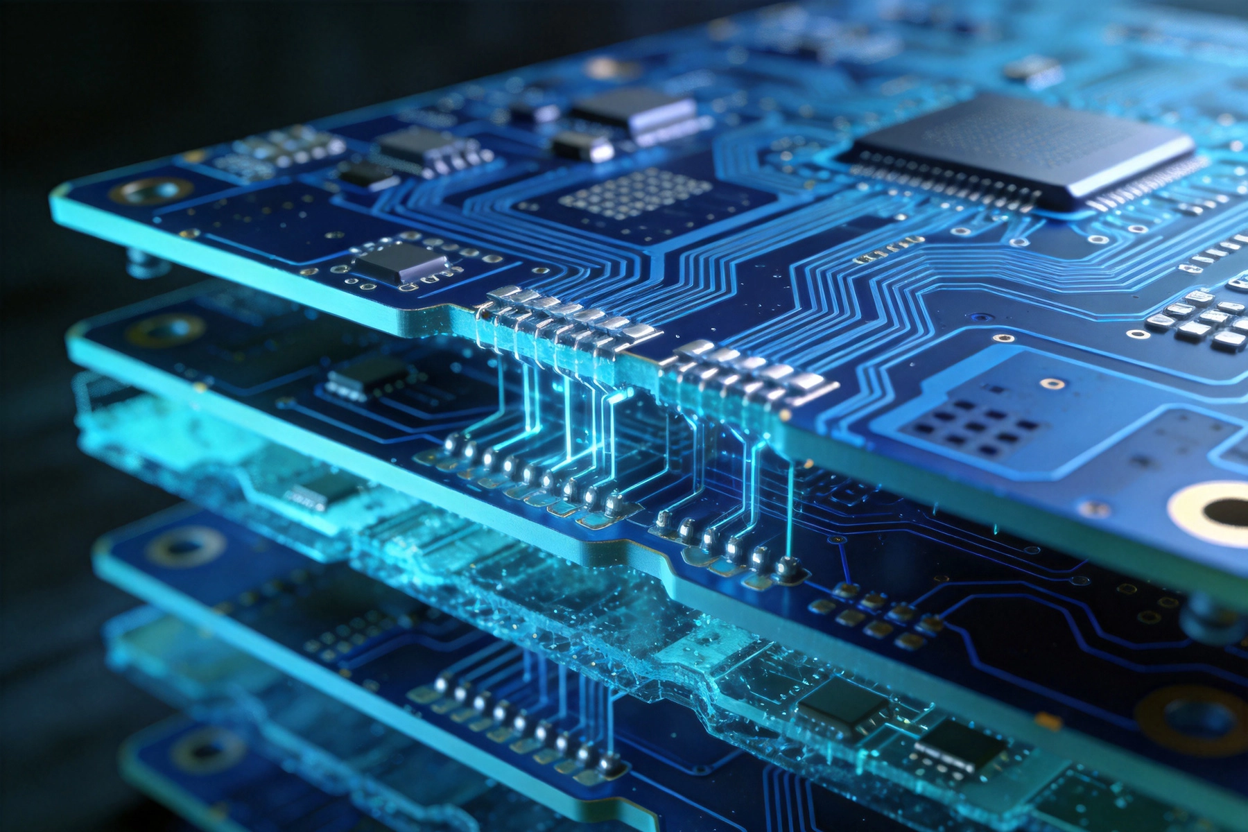
High-Density Interconnect (HDI) printed circuit boards have become the backbone of modern electronics, enabling the compact, high-performance devices we rely on daily. From smartphones to medical implants, HDI technology allows designers to pack mo...
https://www.china-pcbmanufacturer.com/china-multilayer-pcb-manufacturer/understanding-hdi-pcb-stack-ups-best-practices-for-high-density-designs/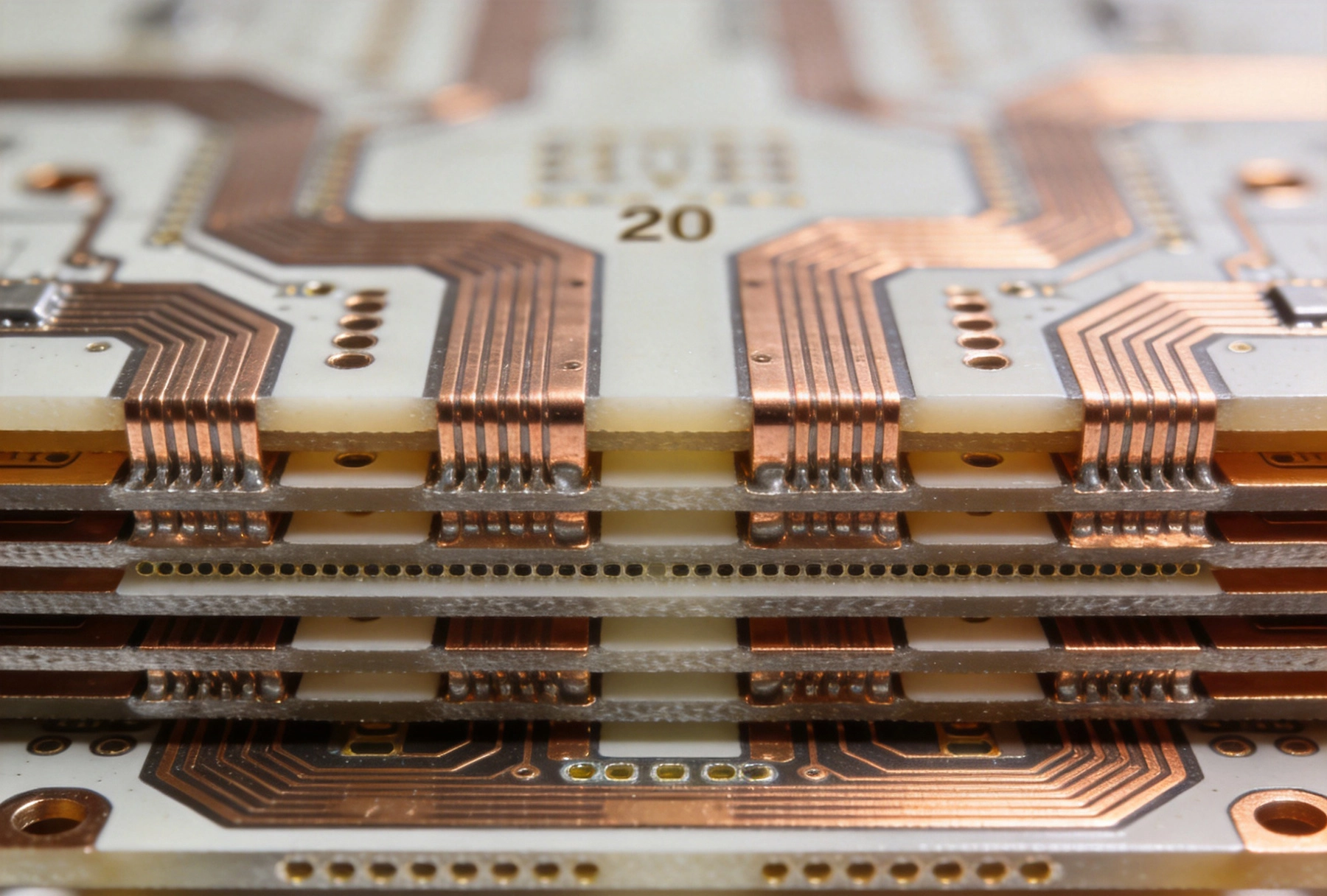
Designing a printed circuit board with 20 or more layers is not simply a matter of stacking more copper onto a familiar structure. As layer count climbs past the ten-layer mark and into the territory of 20, 24, 32, or even 64 layers, every design d...
https://www.china-pcbmanufacturer.com/china-multilayer-pcb-manufacturer/how-to-design-high-layer-count-pcbs-20-layers-for-complex-electronics/