Open Nav

High-density Interconnect (HDI) printed circuit boards have become the backbone of modern electronics, enabling the compact, high-performance devices we rely on daily. From smartphones to medical implants, Hdi Technology allows designers to pack more functionality into smaller form factors while maintaining Signal Integrity and reliability. Understanding Hdi Pcb stack-up design is crucial for engineers working on next-generation electronic products.
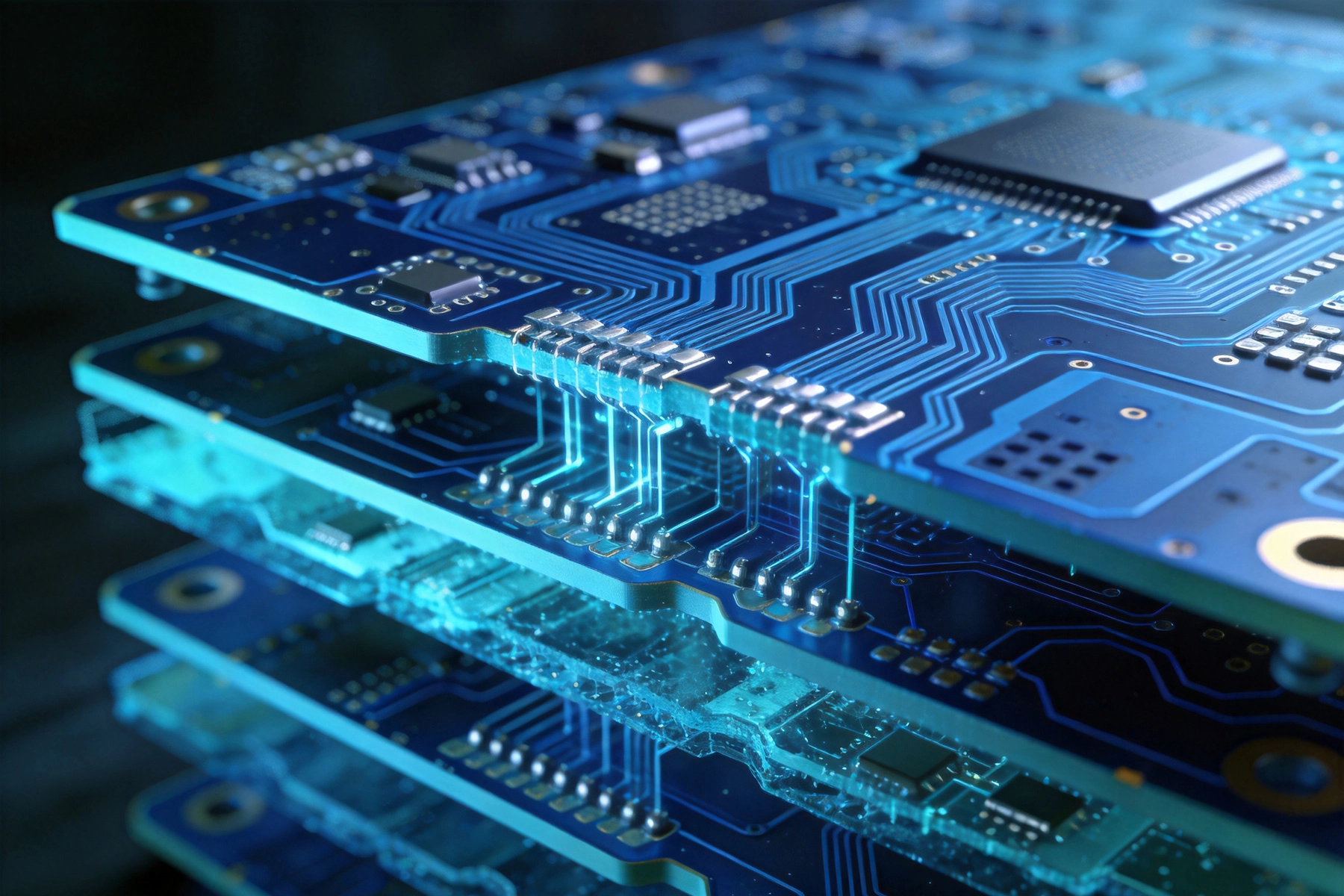
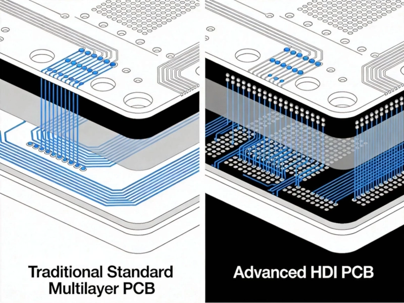
Hdi Pcb refers to a type of Printed Circuit Board that uses higher circuit density compared to traditional boards. The key differentiator lies in the use of Microvias, finer lines, and thinner materials that allow for increased routing density. HDI boards typically feature blind and Buried Vias with diameters of 0.15mm or smaller, and trace widths that are significantly narrower than standard PCB specifications.
The International Printed Circuit Equipment and Materials Association (IPC) defines HDI boards by their via structures and density features. An Hdi Pcb may incorporate any combination of Microvias, advanced build-up processes, and Sequential Lamination cycles that create dense interconnect patterns between layers.
A well-designed Hdi Stack-up balances electrical performance, manufacturability, and cost. The typical HDI board structure consists of core materials, prepreg layers, and copper foils arranged to create the desired electrical characteristics. Standard stack-ups range from 4-layer to 20-layer configurations, with the complexity increasing based on routing density requirements.
The most common HDI configurations include:
The core material thickness directly impacts the board's mechanical strength, Thermal Management, and electrical performance. For HDI designs, cores typically range from 0.1mm to 0.8mm, depending on the overall board thickness requirements. Thinner cores reduce thermal mass during reflow but may require additional support for large components.
Material selection for the core involves balancing dielectric constant (Dk), dissipation factor (Df), thermal conductivity, and CTE (Coefficient of Thermal Expansion). Standard FR-4 remains cost-effective for many applications, while high-speed designs benefit from low-Dk materials such as Rogers or Panasonic Megtron series substrates.
Prepreg (pre-impregnated) materials form the dielectric layers between copper foils in the build-up section. HDI manufacturing typically uses thinner prepregs with resin content carefully controlled to ensure complete fill during lamination. The most common prepreg thicknesses for HDI range from 50 microns to 100 microns.
Resin flow during lamination must be precisely controlled to avoid void formation while ensuring proper fill of the microvia structures. Manufacturers often specify particular prepreg types for HDI applications, and deviation from recommended materials can result in manufacturing failures or reliability issues.
HDI boards utilize three primary via types, each serving specific purposes in the stack-up design:
Through vias traverse the entire board thickness and provide connections between outer layers and internal ground planes. These are the largest vias in HDI designs and establish the foundation for the stack-up.
Buried Vias connect internal layers without extending to either board surface. These vias are formed before the final board lamination and allow for efficient use of internal routing space.
Blind Vias connect an outer layer to one or more internal layers without penetrating the entire board. These are the defining feature of Hdi Technology, enabling high-density routing without consuming space on inner layers.
The aspect ratio (depth to diameter) of microvias critically affects manufacturing yield and reliability. Industry best practice limits aspect ratios to 0.8:1 or lower for laser-drilled microvias. This means a 100-micron diameter via should not exceed 80 microns in depth. Exceeding recommended aspect ratios increases the risk of incomplete copper plating and void formation.
Stacked microvias, where one microvia lands directly on top of another, require additional manufacturing steps and tighter tolerances. While technically feasible, stacked configurations increase cost and reduce manufacturing yield. Skip-via constructions, where microvias land on internal pads rather than other vias, offer improved reliability at the cost of some routing flexibility.
HDI boards frequently carry high-speed signals requiring Controlled Impedance traces. The thinner dielectric layers in HDI stack-ups allow for Controlled Impedance lines with narrower trace widths, but this requires careful calculation and verification. Characteristic impedance depends on trace width, trace thickness, dielectric thickness, and the dielectric constant of the material.
Common impedance targets for HDI designs include 50-ohm single-ended and 100-ohm differential pairs for USB, Ethernet, and high-speed memory interfaces. Design tools with integrated field solvers can calculate required dimensions, but manufacturing tolerances must be considered during the design phase.
Compact HDI designs demand efficient power distribution networks to supply current to numerous components. The reduced trace widths in HDI stack-ups limit current-carrying capacity, making power plane design particularly important. Solid power planes in the core layers provide low-impedance paths for power distribution, while power bumps and microvias connect components to these planes.
Decoupling capacitors must be placed as close as possible to component power pins, with their ground connections returning directly to the plane through shortest-path vias. The inductance of the power path directly impacts switching noise and transient response, making proximity critical for high-speed components.
High component density generates significant thermal loads that must be managed effectively. Hdi Stack-up design influences thermal performance through material selection, via distribution, and copper weight choices. Thermal vias placed under heat-generating components provide paths for heat transfer between layers, while metal core or heavy copper layers can serve as heat spreaders.
The thermal conductivity of Pcb Materials varies widely, from approximately 0.3 W/mK for standard FR-4 to over 1.0 W/mK for high-performance thermal substrates. For applications with sustained high power dissipation, consider thermal prepregs or metal-backed substrates that provide improved heat spreading capabilities.
Inductrial practice increasingly incorporates laminated metal core structures for Thermal Management in HDI designs. These constructions place aluminum or copper cores between dielectric layers, providing efficient heat spreading while maintaining the electrical isolation required for the circuit. However, metal core constructions introduce additional manufacturing complexity and cost that must be justified by the thermal requirements.
HDI manufacturing capabilities continue to advance, with current mainstream production supporting line and space geometries of 75 microns or finer. Advanced facilities can produce 50-micron lines and spaces, with emerging technologies pushing toward even smaller dimensions. Design rules must reflect the capabilities of the chosen manufacturer, and early communication with the fabrication partner is essential.
Feature-to-feature spacing requirements ensure adequate manufacturing margin. Traces should maintain minimum clearances from pads, vias, and other features. These clearances vary by manufacturer but typically range from 50 to 100 microns depending on the technology level and acceptable yield risk.
HDI boards accumulate tolerance stack-up through multiple lamination cycles, making registration control critical. Each Sequential Lamination introduces potential for layer-to-layer misalignment. Design practices that accommodate tolerance accumulation include larger capture pads for blind and buried vias, dog-bone pad structures for via-in-pad designs, and liberal use of cross-sectional references in documentation.
Most HDI manufacturers specify registration tolerances of +/- 50 microns for via-to-pad alignment, but tighter tolerances may be achievable at additional cost. Understanding your manufacturer's specific capabilities and limitations prevents costly design iterations.
While HDI technology enables aggressive Miniaturization, unnecessary complexity drives up costs significantly. Evaluating each layer addition and via structure for necessity prevents over-engineering. Often, a simpler stack-up with optimized routing achieves the same functional density at lower cost than a complex high-layer-count design.
Panel utilization affects cost substantially. Designs that utilize standard panel sizes efficiently reduce per-board costs. Avoiding oversized boards, excessive margins, and non-standard shapes contributes to cost-effective manufacturing.
Standard FR-4 materials offer the lowest cost path for HDI production, with performance adequate for many applications. Specialty materials such as low-loss laminates increase cost by 2x to 5x depending on the specific product. Justifying material upgrades requires clear performance requirements that standard materials cannot meet.
Volume production typically reduces per-board costs, but NRE (non-recurring engineering) charges for HDI can be substantial. Prototype and low-volume runs may carry premium pricing that decreases with quantity. Planning for volume production from the initial design phase allows optimization for cost-effective manufacturing.
Several recurring issues plague HDI PCB designs and can be avoided with proper planning. Using excessive aspect ratios for microvias leads to plating failures and field returns. Inadequate capture pad sizes for blind and buried vias create reliability problems under thermal cycling. Ignoring the coefficient of thermal expansion mismatch between materials and components causes solder joint failures over time.
Failure to verify stack-up impedance calculations with the manufacturer results in boards that meet design intent but miss impedance targets. Designing beyond the manufacturer's true capabilities creates unrealistic expectations and manufacturing delays. Always validate stack-up designs with qualified fabrication partners before releasing to production.
Mastering HDI Pcb Stack-up Design requires balancing electrical performance, thermal management, manufacturability, and cost. Understanding the fundamental elements—layer structures, microvia implementation, and material selection—provides the foundation for successful high-density designs. Following best practices for Signal Integrity, thermal management, and manufacturing collaboration ensures that designs perform reliably in their intended applications.
As electronic devices continue demanding greater functionality in smaller packages, HDI technology remains essential for competitive product development. Investing in proper HDI stack-up design practices early in the product development cycle prevents costly revisions and ensures successful product launches.
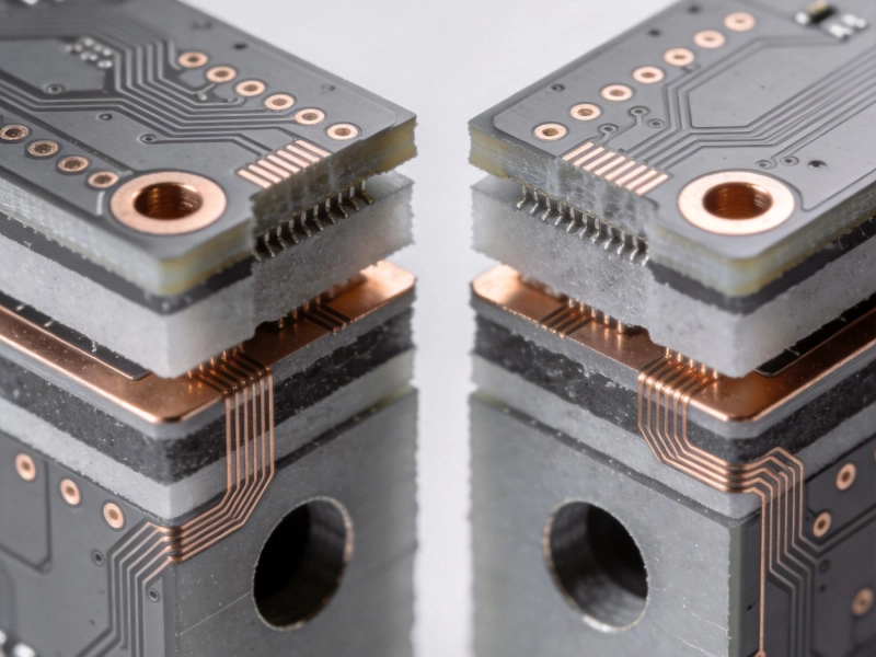
Microvias vs. Through-Holes: Choosing the Right Tech for Your Multilayer BoardAugust/06/2026
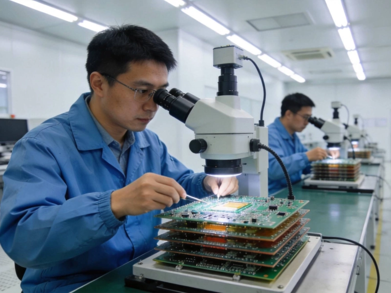
How We Ensure Quality Control in Multilayer PCB LaminationAugust/08/2026
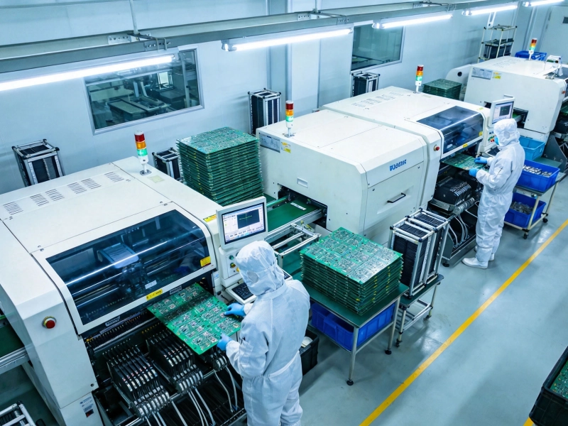
Behind the Scenes: A Tour of Our State-of-the-Art PCB Factory in ChinaMay/19/2026
How to Design High-Layer Count PCBs (20+ Layers) for Complex ElectronicsSeptember/08/2026
Durability Requirements for Industrial IoT PCBs: Ensuring Reliability in Harsh EnvironmentsSeptember/03/2026
What Are Multilayer PCBs? A Complete Guide from ChinaMay/18/2026
Why Your LED Lighting Project Needs an Aluminum PCBOctober/14/2026
HDI PCB vs Standard PCB: Key Differences ExplainedMay/13/2026