
Designing a Printed Circuit Board with 20 or more layers is not simply a matter of stacking more copper onto a familiar structure. As layer count climbs past the ten-layer mark and into the territory of 20, 24, 32, or even 64 layers, every design decision carries compounded consequences. Signal Integrity, power delivery, thermal performance, and manufacturing yield all intersect in ways that do not appear in simpler boards. Engineers who have mastered four-layer or six-layer designs often find that intuition built at those counts leads them astray when the stack-up doubles or triples in complexity.
This guide walks through the critical engineering decisions that drive success in high-layer count Pcb Design, from stack-up planning and layer allocation to via strategy, impedance control, and the manufacturing realities that constrain what can actually be built at scale.
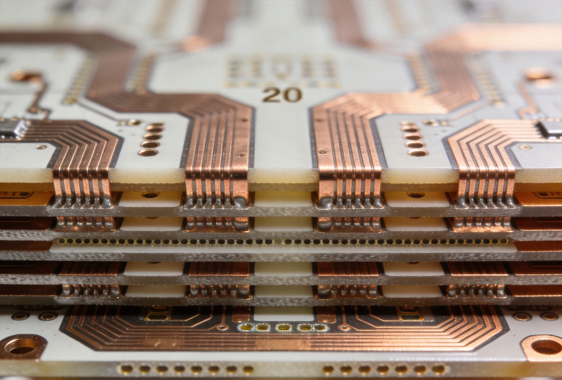
A four-layer board has two signal layers and two planes. An eight-layer board might distribute four signal layers across two reference planes on each side. At 20 layers and beyond, you are managing dozens of signal layers, multiple isolated power domains, high-speed differential pairs, analog circuits, and a power distribution network that must serve components drawing currents ranging from microamps to tens of amps simultaneously.
The difference is not just quantitative. At high layer counts, the interactions between layers become the dominant design challenge. A signal route on layer 12 might couple capacitively to a switching power rail on layer 13. A via connecting layer 3 to layer 18 creates a long stub that acts as a resonant stub at microwave frequencies. These effects do not exist at low layer counts, which is why different design methodologies and verification workflows become essential.
The stack-up is the single most consequential decision in high-layer count Pcb Design. Done well, it simplifies every downstream problem. Done poorly, no amount of routing optimization or simulation can fully compensate.
The basic principle is symmetric construction. A balanced stack-up places an equal number of layers above and below the board center plane. This minimizes bow and twist during lamination and reflow, which is critical at 20+ layers where cumulative stress from mismatched copper densities can cause dimensional instability large enough to crack BGA solder joints or delaminate inner layer connections.
For a 20-layer board, a typical symmetrical stack-up might look like this:
Notice the repeating pattern of signal-ground and power-ground pairs. This provides every signal layer with an adjacent reference plane, minimizing loop area and controlling return current paths. The specific arrangement depends on the board's primary function, but the principle of consistent reference plane adjacency applies universally.
Core and prepreg thicknesses must be chosen to meet impedance requirements while remaining within the manufacturing tolerances of the PCB fabricator. Standard FR-4 cores are readily available up to about 0.5mm thickness. Beyond that, high-Tg or specialized substrates become necessary. Always validate stack-up choices against the fabricator's capabilities before finalizing the design.
A common mistake in high-layer count design is over-allocating signal layers at the expense of plane layers. Plane layers serve three critical functions: providing a low-impedance return path for signals, distributing power to components across the board, and acting as an effective shield against external interference. Reducing plane count to squeeze in more routing channels degrades all three.
A reliable rule of thumb for complex digital boards is to allocate approximately one plane layer for every two signal layers. In a 20-layer board, this means roughly 13 signal layers and 7 plane layers, or a similar distribution. The exact split depends on the density of the design and whether multiple isolated power rails require dedicated planes.
Split planes, where a single layer carries multiple isolated voltage domains, are common in high-layer designs but require careful management. Each split must be clearly documented, and signals crossing between voltage domains must be routed through explicit level-shifting components rather than relying on the plane boundary to provide isolation. Designers who treat split planes as simple isolation zones frequently create unintentional discontinuities in the return current path.
Via design becomes exponentially more critical as layer count increases. Through-hole vias that connect layer 1 to layer 20 create long stubs that act as quarter-wave antennas at high frequencies, causing resonances that corrupt Signal Integrity. Several via technologies address this problem.
Blind Vias connect an outer layer to one or more inner layers without penetrating the full board depth. They reduce stub length and free up routing density on outer layers, but they require Sequential Lamination processes that add cost and limit the number of Blind Via steps a fabricator can reliably produce.
Buried Vias connect only inner layers and are invisible from the board surface. They enable high-density interconnections without consuming surface routing real estate, but they require the most complex manufacturing sequences and are typically the most expensive via type per connection.
Back-drilling removes the unused portion of a through-hole via stub after plating by drilling from the surface to the target layer. It is a cost-effective alternative to blind and Buried Vias for designs where the stub length is the primary concern. Most advanced PCB Fabrication shops support back-drill tolerances down to 0.15mm on controlled depth.
Microvias, typically laser-drilled with diameters of 0.05mm to 0.15mm, are the backbone of HDI (High-density Interconnect) designs. In 20+ layer boards, microvia-in-pad and stacked microvia structures allow routing density that would be impossible with mechanical drill sizes alone. However, microvia reliability at high layer counts requires careful attention to aspect ratio and plating quality, particularly in thermal cycling environments.
The practical recommendation is to use the simplest via technology that meets the design requirements. Adding blind, buried, or microvia structures beyond what the design genuinely needs increases cost and reduces manufacturing yield. Reserve these technologies for the specific high-density zones where routing density or signal performance demands them.
In high-layer count boards, the Power Delivery Network (PDN) spans dozens of layers and must supply clean, stable voltage to components that may be drawing hundreds of amps at low voltage (such as processors and FPGAs) alongside micro-power analog circuits. The PDN design must address three interrelated problems: IR drop, switching noise, and concurrent switching noise.
IR drop is the voltage lost as current flows through the plane resistance from the VRM to the component. At high currents, even milliohm-level plane resistance causes measurable voltage sag at the load. The solution is to provide sufficient copper weight on power planes. Many 20+ layer server and AI accelerator boards use 2oz or 3oz copper on power planes, with some designs going to 4oz or heavier for the highest current domains.
Switching noise arises when fast transients in the load current couple into the power plane and radiate into adjacent signal layers. Decoupling capacitors placed near the component pins provide high-frequency current local to the load, but the planes themselves must be designed with low inductance. This is achieved by minimizing the dielectric spacing between power and ground plane pairs, typically 2-4 mils in high-performance stack-ups.
Concurrent switching noise, where multiple output drivers switch simultaneously and draw peak currents that exceed the decoupling capacity, requires careful PDN impedance analysis across the full frequency range from DC to the Nyquist frequency of the fastest switching edge. Simulation tools like S-parameter extraction and time-domain analysis are nearly essential for 20+ layer designs with GHz-class processors.
Signal integrity in high-layer count boards depends on three pillars: Controlled Impedance, consistent return paths, and crosstalk management.
Controlled Impedance traces must maintain their characteristic impedance within the tolerance specified by the signal standard, typically plus or minus 10% for single-ended traces and plus or minus 5% for differential pairs. In a 20-layer stack-up, achieving tight Impedance Tolerance requires accurate dielectric constant values for the substrate materials, precise control of trace geometry, and consideration of the proximity effects from adjacent copper features.
Return current paths are often the most overlooked aspect of high-layer count signal integrity. Every signal needs a reference plane. When a signal transitions between layers through a via, the return current must also transition. If the reference plane changes at the via, the loop area spikes and radiated emissions increase. Design practice is to place ground stitching vias within 1mm of any signal via that changes reference planes, providing a low-inductance path for the return current to follow the signal.
Crosstalk between adjacent signal traces becomes more challenging as routing density increases. In 20-layer boards, traces on non-adjacent layers can still couple through the shared reference plane, particularly when high-speed signals run parallel to each other over long distances. Differential routing with adequate pair-to-pair spacing, ground guard traces alongside sensitive nets, and layer-to-layer orthogonal routing directions all contribute to crosstalk control.
High-layer count boards pack significant power density into a relatively constrained volume. Thermal Management must be considered from the stack-up stage, not added as an afterthought.
The primary thermal paths in multilayer boards are through thermal vias to copper planes and surface-level heat spreaders. For boards with 20+ layers, internal copper planes can serve as effective heat spreaders if they are continuous under the thermal load. Thermal relief patterns in plane layers, while necessary for soldering, also restrict thermal conductivity. The design must balance solderability requirements against the need for unobstructed copper thermal paths.
Components with high power dissipation, such as processors, GPUs, and power regulators, benefit from thermal via arrays placed directly beneath the thermal pad. Via-in-pad with filled or capped plating ensures that the thermal path is not interrupted by voids in the barrel plating.
For extreme power densities, metal-core or metal-backed substrates, hybrid stack-ups combining standard laminates with metal heat-spreading cores, or even liquid cooling integration through embedded micro-channel structures become relevant. These approaches add significant cost and manufacturing complexity, but for boards in AI accelerators, Power Electronics, and aerospace applications, they are often unavoidable.
Designing for 20+ layers requires a close partnership between the design team and the PCB fabricator. Manufacturing capabilities and limitations directly shape what is achievable.
Layer-to-layer registration becomes increasingly demanding as layer count grows. At 20+ layers, registration tolerances of 0.05mm or tighter are required to maintain annular ring integrity on the smallest vias. This demands sophisticated imaging and lamination equipment that not all manufacturers possess.
Minimum Trace Width and spacing capabilities vary by manufacturer and by the number of layers. Standard capabilities for a 20-layer board are typically 0.1mm (4 mil) lines and spaces, with tighter capabilities available at premium pricing. Designers must verify their fabricator's specific capabilities for the target layer count before finalizing the layout.
Aspect ratio, the ratio of board thickness to smallest drill diameter, limits the minimum via size for through-hole connections. A board that is 3.2mm thick with 0.25mm minimum drill size has an aspect ratio of 12.8:1, which is at the edge of many manufacturers' capabilities. Designers may need to accept larger through-hole sizes or work with the fabricator to optimize the drill schedule.
Lamination pressure and temperature cycles can cause inner layer shift, where the copper features on one layer shift relative to adjacent layers during the lamination process. High-layer count designs use design features such as tooling holes, fiducial marks, and anti-shift lands to assist with layer-to-layer alignment during manufacturing. The fabricator should be consulted on the specific fiducial and tooling requirements for the target production facility.
Many 20+ layer boards are built for high-speed digital applications: AI accelerators, networking equipment, data center hardware, and test and measurement instruments. These applications demand tight impedance control on Transmission Line structures.
For single-ended traces carrying high-speed signals, the target impedance is typically 50 ohms. Differential pairs are usually targeted at 85-100 ohms depending on the signal standard. Achieving these values consistently across a 20-layer board requires running impedance calculations for each signal layer, not just assuming that all layers will match the same stack-up parameters.
Trace geometry, including width, thickness, and height above the reference plane, must be modeled accurately. The effective dielectric constant of the substrate material, which varies with resin content and glass weave style, introduces uncertainty that must be accounted for in the tolerance budget. Many fabricators offer impedance-controlled fabrication with measured coupon verification, where test structures on the panel are measured after production to confirm impedance targets were met.
Route topology matters as much as trace geometry. 90-degree bends in high-speed traces create discontinuities. Mitered bends or rounded corners reduce reflections. Pad-to-line transitions at component connections and at layer change points introduce capacitance that must be accounted for in high-frequency designs. Careful routing practices, including avoiding via stubs on critical nets through back-drilling, form an integral part of impedance control at this level of complexity.
A 20+ layer board generates a corresponding volume of documentation that must accurately communicate the design intent to the fabricator and assembly house. Generic fabrication notes are insufficient at this complexity level.
The fabrication drawing should include a full stack-up table listing each layer's name, thickness, material, copper weight, and any special requirements such as impedance targets or plane clearance specifications. Via specifications should detail the type (through, blind, buried, back-drill), dimensions, and the specific layers each via connects. Any non-standard materials, surface finishes, or special processes should be called out explicitly with references to the appropriate specifications.
Design rule checks must be run and verified before handoff. This includes not just standard DRC checks but also specific verifications for impedance-controlled nets, thermal relief connections, antipad clearance, and via-to-via spacing. Many high-layer count designs benefit from additional custom checks written for the specific PDN and routing rules of the project.
Designing a 20+ layer PCB is a systems engineering challenge that requires simultaneous attention to stack-up architecture, signal and power distribution, Thermal Management, and manufacturing constraints. The principles are well-established, but their application at high layer counts demands careful analysis, accurate simulation, and close collaboration with fabrication partners.
The engineers who produce the most reliable high-layer count designs are those who engage their fabricator early, validate stack-up decisions against real manufacturing data, and resist the temptation to push routing density beyond what the Manufacturing Process can consistently deliver. In complex electronics, the difference between a design that works reliably at scale and one that delivers intermittent field failures often comes down to decisions made in the stack-up planning stage.
At scale, a 20-layer board typically costs 2.5 to 4 times more than a comparable 10-layer board, depending on the minimum feature sizes, via technologies, and material specifications. The cost premium is driven primarily by the additional lamination cycles, more complex drill schedules, and tighter registration tolerances required for high-layer count boards.
Back-drilling is generally preferred when cost is the primary constraint and the design can tolerate the slightly larger via landing pad required for controlled-depth drilling. Blind and buried vias are chosen when minimizing stub length on high-frequency signals is critical and the design budget can support Sequential Lamination processes. Many high-performance 20-layer designs use a combination of both technologies in different zones of the board.
Commercially available PCB Fabrication supports layer counts up to 64 layers with standard processes, and some specialty manufacturers can produce boards with 100 or more layers using advanced techniques. Above 32 layers, the cost escalation and manufacturing complexity become substantial, and alternative approaches such as modular or multi-chip assembly are often considered.
Thicker boards accommodate more layers more easily but face challenges with via aspect ratio, signal integrity (longer via stubs), and thermal management. Thin boards offer better electrical performance for high-speed signals but have limited space for high-current planes. For most 20-layer applications, a board thickness between 2.0mm and 3.2mm provides a practical balance of these trade-offs.
At minimum, a PCB design tool with robust stack-up management, impedance calculation, and design rule checking is required. For complex designs, electromagnetic simulation tools for signal integrity analysis, thermal simulation for power density assessment, and PDN analysis tools are strongly recommended. Close coordination with the fabricator through ODB++ or IPC-2581 data exchange formats ensures that manufacturing constraints are properly communicated.
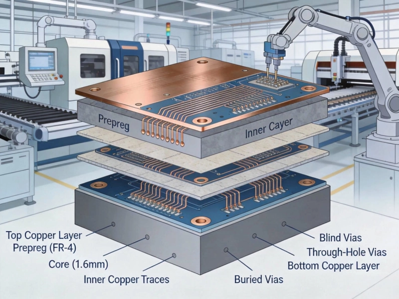
What Are Multilayer PCBs? A Complete Guide from ChinaMay/18/2026
Durability Requirements for Industrial IoT PCBs: Ensuring Reliability in Harsh EnvironmentsSeptember/03/2026
How We Ensure Quality Control in Multilayer PCB LaminationAugust/08/2026
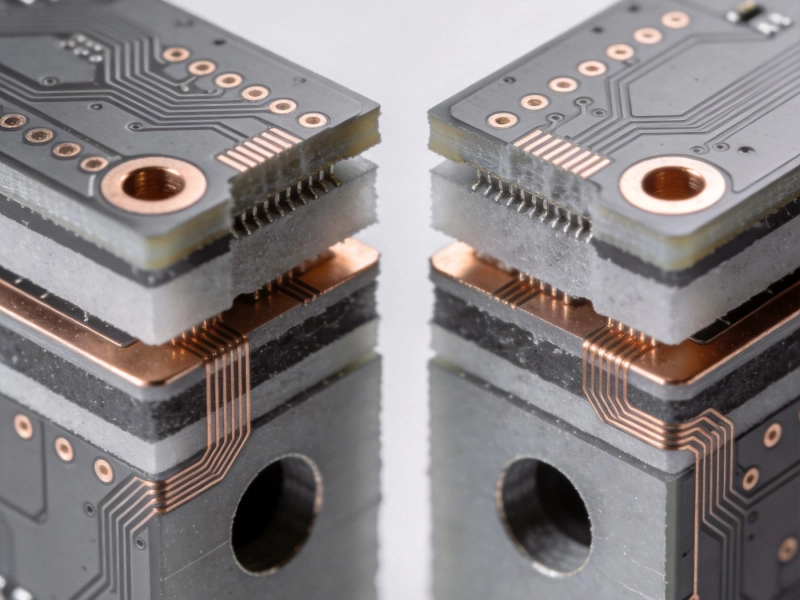
Microvias vs. Through-Holes: Choosing the Right Tech for Your Multilayer BoardAugust/06/2026

Behind the Scenes: A Tour of Our State-of-the-Art PCB Factory in ChinaMay/19/2026

Understanding HDI PCB Stack-ups: Best Practices for High-Density DesignsJuly/18/2026
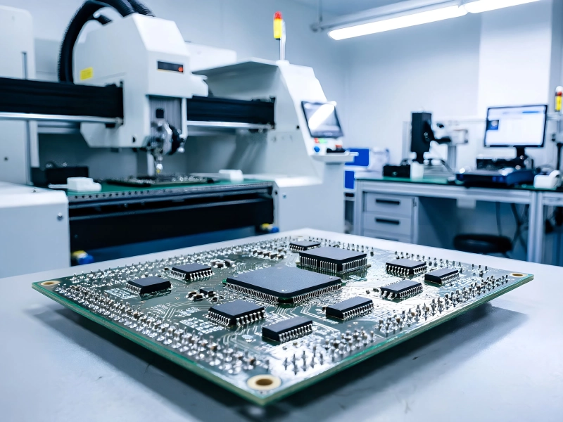
Top 10 DFM Mistakes to Avoid Before Sending Files to China for SMT AssemblyJuly/15/2026
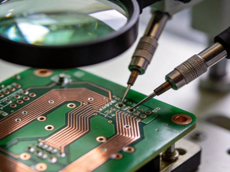
How to Verify the Quality of a PCB Prototype Before Mass ProductionOctober/13/2026