Open Nav
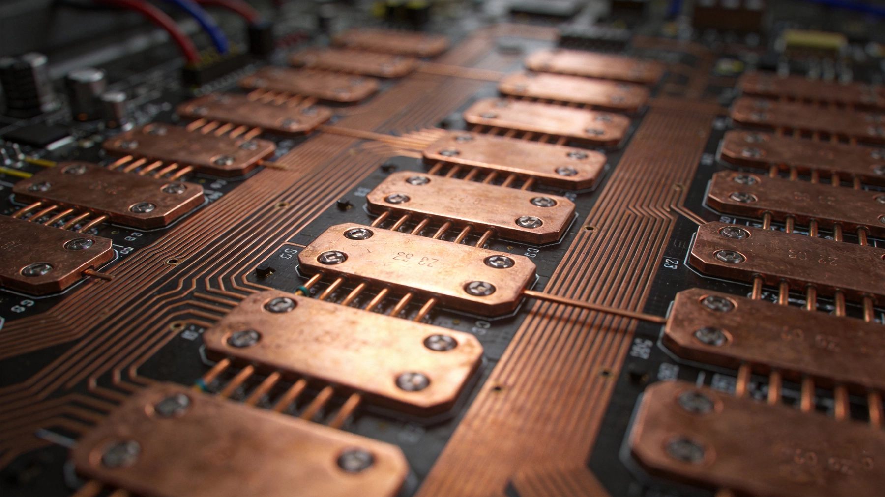
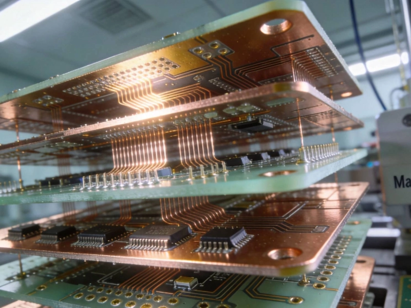
Industrial control systems demand reliable power distribution, robust current handling, and thermal stability under demanding operating conditions. These requirements often exceed what standard PCB constructions can provide, driving designers toward heavy copper architectures that accommodate high current flow while maintaining circuit integrity. Heavy copper PCBs—those with copper weights significantly beyond the standard 1oz per square foot specification—enable industrial control boards to handle the substantial currents and thermal loads that define power electronics applications.
The distinction between standard and heavy copper isn't merely quantitative. Standard PCB constructions use one ounce copper (approximately 35 micrometers) as a baseline, adequate for signal traces and low-power distribution. Heavy copper typically refers to 3oz, 4oz, or greater copper weights—sometimes reaching 10oz or beyond for extreme applications. These increased copper thicknesses fundamentally change both electrical and thermal performance, enabling board-level designs previously requiring bus bars or discrete wiring solutions.
This article examines why heavy copper PCBs have become essential for high-voltage industrial control applications, the engineering principles underlying their design, manufacturing considerations, and practical guidance for implementing heavy copper in industrial control board designs.
Industrial control boards distribute power from primary sources to various loads: motor drives, contactors, sensors, and logic circuits. Each distribution path must carry specific current levels without excessive voltage drop or thermal rise. Understanding current requirements establishes the foundation for heavy copper specification.
Power distribution efficiency imposes voltage drop limits:
System Voltage Budget: Most industrial systems allocate specific voltage tolerances for distribution—typically 3-5% of nominal voltage. For a 24V control system, this permits only 0.7-1.2V drop across the entire distribution network before reaching loads.
Trace Resistance Impact: Standard 1oz copper traces exhibit approximately 0.5 milliohms per square inch of cross-section. For a trace carrying 10A over 6 inches, voltage drop could exceed acceptable limits, particularly at lower system voltages.
Load Performance Degradation: Loads operating below nominal voltage deliver reduced performance. Motors run slower, solenoids provide weaker actuation, and electronic loads may reset or malfunction. Heavy copper reduces these losses proportionally to the increase in cross-sectional area.
Current flow generates heat according to power dissipation principles:
Power Dissipation Formula: Heat generated equals I²R, where R is trace resistance. Doubling current quadruples heat generation. This non-linear relationship makes current density management critical for thermal control.
Ambient Temperature Stacking: Industrial environments often reach elevated temperatures—control cabinets with significant internal heat from components, processes, or limited ventilation. Trace heating adds to ambient temperature, potentially exceeding component ratings or creating unsafe surface temperatures.
Reliability Impact: Every 10°C increase in operating temperature approximately halves component lifetime. Traces operating near thermal limits accelerate degradation of solder joints, laminates, and adjacent components.
Heavy copper improves current carrying through fundamental electrical principles. Understanding these principles enables accurate specification and optimization.
Copper resistance scales inversely with cross-sectional area:
Area Proportionality: A 3oz copper trace has three times the cross-sectional area of 1oz copper, reducing resistance to approximately one-third. This reduction directly decreases both voltage drop and I²R heating.
Temperature Coefficient: Copper resistance increases with temperature—approximately 0.4% per °C. Lower operating temperature from reduced heating creates a beneficial cycle where heavy copper stays cooler, maintaining lower resistance than thermally-stressed lighter copper.
Skin Effect at High Frequencies: AC current tends toward conductor surfaces, reducing effective cross-section. At industrial frequencies (50/60Hz), skin effect is negligible. For switching power supplies with higher frequency components, heavy copper's benefit diminishes, though external plating maintains some advantage.
Beyond reducing self-heating, heavy copper improves heat dissipation:
Thermal Spreading: Thick copper spreads heat laterally across the board surface, distributing thermal energy to larger areas where it can dissipate through convection and radiation.
Via Thermal Mass: Heavy copper through-hole plating provides thermal vias with substantially greater conductivity than standard plating, enabling heat transfer between layers or to external heatsinks.
Plane Connectivity: Power planes in heavy copper construction provide both electrical distribution and thermal spreading in a single structure, simplifying design while improving performance.
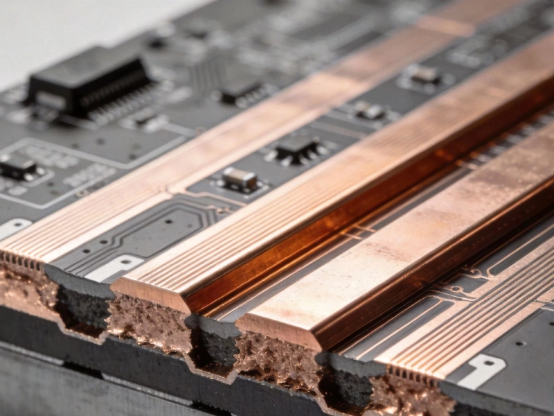
Heavy copper Pcb Manufacturing requires specialized processes beyond standard fabrication. Understanding these capabilities helps designers specify achievable requirements and recognize capable manufacturing partners.
Fabrication capabilities define specification boundaries:
Standard Heavy Copper Range: Most PCB fabricators handle 3oz to 6oz copper routinely. This range suits the majority of industrial control applications without requiring specialized equipment.
Extended Heavy Copper: Capabilities up to 10oz-12oz exist at specialized facilities. These constructions require modified plating equipment, adjusted etching processes, and careful process control.
Extreme Heavy Copper: Ultra-thick copper (20oz+) represents a specialized niche for bus bar replacements or extremely high current applications. These boards approach hybrid constructions combining Pcb Technology with discrete bus bar elements.
Heavy copper processing introduces manufacturing complexities:
Etch Factor Limitations: Chemical etching becomes more challenging with thicker copper. Trace sidewalls show greater taper, affecting impedance control and feature resolution. Experienced fabricators optimize etch chemistry and compensation to maintain acceptable feature geometry.
Plating Uniformity: Electroplating thickness uniformity becomes more difficult on heavy panels. Edge-to-center variation and panel-to-panel consistency require careful process control and measurement.
Registration Accuracy: Thicker copper layers affect lamination pressure distribution and dielectric thickness control. Registration between layers requires compensation for the increased mass and different thermal characteristics.
Heavy copper often requires compatible base materials:
High Tg Materials: Elevated glass transition temperature (Tg) materials—typically Tg170 or higher—maintain mechanical stability during thermal processing of heavy copper boards, which experience greater thermal mass and processing stress.
Thermal Conductivity Options: For applications with significant heat dissipation requirements, metal-core substrates or ceramic-filled materials provide improved thermal conductivity beyond standard FR-4.
Prepreg Compatibility: Bonding ply (prepreg) selection must accommodate heavy copper processing requirements. Higher flow prepregs fill gaps between heavy copper features while maintaining controlled dielectric thickness.
Effective heavy copper design integrates electrical, thermal, and manufacturing considerations from concept through production.
Heavy copper geometry differs from standard design:
Width Calculation: Trace width for current carrying depends on copper weight, allowable temperature rise, and adjacent copper coverage. Standard IPC formulas require modification for heavy copper applications. Designers should use manufacturer-supplied current capacity tables specific to their heavy copper capabilities.
Spacing Requirements: High-voltage applications impose minimum spacing requirements based on voltage potential, contamination risk, and safety standards. Heavy copper features may require increased spacing compared to thin-trace designs due to different conformal coating behavior and surface geometry.
Manufactureable Geometry: Trace widths must accommodate fabrication capabilities—minimum achievable width increases with copper weight. Designers should verify minimum feature specifications with intended manufacturers early in the design process.
Vias present particular challenges for current carrying:
Via Current Capacity: Standard microvias cannot carry substantial current. Heavy copper boards require larger through-hole vias with substantial plating thickness to transfer current between layers. Thermal relief patterns connect heavy copper planes to via barrels.
Filling and Plating: For the highest current applications, vias may be filled with copper or conductive paste and planarized, creating low-resistance connections between layers. This approach adds cost but provides current capacity approaching solid copper.
Via-in-Pad: Connection directly to component pads (via-in-pad) eliminates thermal relief resistance but complicates assembly. Solder wicking into vias can affect joint reliability if not properly managed.
Heavy copper boards integrate with broader thermal strategies:
Thermal Via Arrays: Regular patterns of thermally-connected vias transfer heat between layers or to external heatsinks. Thermal via design requires attention to via density, thermal relief geometry, and connection to spreading planes.
Heatsink Integration: Boards may bolt directly to heatsinks using thermal interface materials. Heavy copper power planes provide low-resistance thermal paths to these external cooling surfaces.
Component Thermal Shading: Sensitive components benefit from shielding against localized heating from high-current traces. Heavy copper areas can provide thermal isolation when properly positioned.
Heavy copper PCBs appear across diverse industrial control applications, each with specific requirements that influence design approaches.
Motor control presents combined high current and thermal challenges:
Inverter Stage Power Distribution: MOSFET or IGBT switching stages distribute substantial current to motor windings. Heavy copper bus bars and power planes handle 10A to 100A+ currents with controlled temperature rise.
Gate Drive Isolation: Gate drive circuits require isolated low-current distribution but benefit from heavy copper thermal management in adjacent power stages.
Current Sensing: Shunt resistors for current measurement benefit from heavy copper connections to minimize temperature effects on resistance values.
Power supply boards exemplify heavy copper requirements:
Rectifier Stage: AC-DC conversion stages carry substantial currents at line potentials. Heavy copper bridges and planes distribute this power efficiently.
Output Distribution: Multiple output rails require careful power plane design to maintain isolation while providing adequate current capacity for each output.
Magamp Control: Magnetic amplifier control windings and saturable reactors in high-current power supplies benefit from heavy copper construction.
PLC systems often combine logic and power on single boards:
I/O Module Power Rails: Input/output modules drive external loads requiring higher current than logic circuits. Field device power distribution uses heavy copper to maintain voltage regulation.
Backplane Connections: High-current backplane distribution for rack-mounted PLC systems uses heavy copper connectors and traces to minimize distribution losses.
Relay Driver Boards: Coil currents for industrial relays—particularly larger contactors—benefit from heavy copper distribution to prevent voltage drop affecting relay operation.
Heavy copper Pcb Production requires manufacturing partners with specific capabilities and experience.
Evaluate heavy copper capabilities systematically:
Copper Weight Range: Confirm the manufacturer handles your specific copper weight requirement. Ask about their standard production versus specialty capabilities.
Feature Resolution Limits: Understand minimum trace/space capabilities at your target copper weight. Heavy copper reduces achievable feature density.
Multi-Layer Heavy Copper: Combining heavy copper with multi-layer construction requires advanced capabilities. Verify experience with your specific layer count and copper weight combination.
Quality systems for heavy copper require particular attention:
Process Control Documentation: Heavy copper processing requires tighter process control than standard construction. Request evidence of controlled processes and inspection procedures.
Electrical Testing: Bare board testing must account for heavy copper characteristics. Discuss their test methodology and acceptance criteria.
Material Certification: Base material and Copper Foil certifications should document specifications and lot traceability.
Design support capabilities vary significantly:
DFM Review Specificity: Heavy copper DFM differs from standard review. Confirm the manufacturer provides specific guidance for heavy copper applications.
Thermal Analysis Capability: Some manufacturers offer thermal simulation or measurement services that help optimize heavy copper design.
Prototype Support: Understanding how prototypes will be processed helps anticipate production challenges before volume commitment.
Heavy copper construction carries premium costs compared to standard Pcb Fabrication. Understanding these cost drivers enables informed design decisions.
Heavy copper pricing reflects manufacturing complexity:
Material Costs: Copper represents a significant portion of heavy copper board cost. Higher copper weight directly increases raw material expense.
Process Time: Plating, etching, and cleaning processes require longer cycle times for heavy copper. Equipment utilization decreases as processing time increases.
Yield Impact: Heavy copper processing presents greater yield challenges than standard construction. Higher defect rates translate to higher unit costs.
Tooling Modifications: Some heavy copper processes require custom tooling—specialized stencils, plating anodes, or etching fixtures—that add non-recurring engineering costs.
Cost premiums may be justified by performance benefits:
System Cost Reduction: Heavy copper can eliminate discrete bus bars, wire harnesses, or additional thermal management components that add cost and complexity.
Reliability Improvement: Reduced operating temperatures and lower connection resistance improve field reliability, reducing warranty costs and customer satisfaction impact.
Size and Weight Optimization: Heavy copper enables smaller board footprints than equivalent standard copper construction, reducing enclosure size and material costs downstream.
Manufacturing Simplification: Consolidated power distribution on PCB versus discrete wiring reduces assembly cost and improves manufacturing consistency.
Heavy copper PCBs represent an essential technology for high-voltage industrial control applications where standard constructions cannot provide adequate current handling, thermal management, or reliability margins. The physics underlying heavy copper benefits—reduced resistance, improved thermal spreading, and enhanced current capacity—translate directly to practical performance improvements in industrial control systems.
Designing with heavy copper requires understanding manufacturing capabilities, material interactions, and thermal management integration. Designers who grasp these principles can specify achievable requirements while optimizing board performance. Manufacturing partners with demonstrated heavy copper expertise provide invaluable support in translating designs into reliable products.
While heavy copper construction carries cost premiums compared to standard Pcb Fabrication, the total system value often justifies the investment. Eliminating discrete wiring, reducing enclosure size, improving reliability, and simplifying assembly contribute to cost-effective solutions despite higher board-level expense.
Industrial control applications continue demanding more from power distribution systems—higher currents, better thermal performance, and improved reliability. Heavy copper Pcb Technology provides the building blocks for these demanding solutions, enabling designs that were previously impractical or impossible using standard constructions. Understanding and applying heavy copper principles positions industrial control designers to meet these escalating requirements effectively.
Heavy copper typically refers to copper weights of 3oz per square foot and above. Standard PCB construction uses 1oz copper (approximately 35 micrometers). Heavy copper commonly ranges from 3oz to 6oz for most industrial applications, with extended capabilities up to 10oz-12oz for extreme requirements.
Heavy copper provides thermal benefits through two mechanisms. First, lower resistance means less I²R heating for the same current. Second, thicker copper spreads heat more effectively across the board surface to areas where it can dissipate through convection and radiation. Combined with thermal vias, heavy copper enables effective heat transfer to external heatsinks.
Heavy copper boards can generally use standard assembly processes with some considerations. Higher thermal mass requires adjusted reflow profiles. Component pads may need thermal relief design to prevent cold joints. Solder paste volume may require adjustment for flat surfaces. Experienced assembly providers understand these adaptations.
Current capacity depends on copper weight, trace width, allowable temperature rise, and adjacent copper coverage. As a rough reference, 3oz copper at 10°C rise carries approximately 15-20A per inch of width. Designers should use manufacturer-provided current capacity data specific to their heavy copper capabilities.
No. Many industrial control boards carry only signal-level currents where standard copper weight suffices. Heavy copper becomes necessary when current requirements exceed approximately 3-5A continuously, thermal management is critical, or voltage drop constraints require lower trace resistance. Evaluating actual requirements prevents unnecessary cost.
Tags: Heavy Copper Pcb, high voltage industrial board, Power Electronics Pcb, current carrying capacity, industrial control systems, thermal management PCB, thick copper fabrication
What is Heavy Copper PCB? Complete Guide from China ManufacturerMay/18/2026

What is Rigid-Flex PCB? Complete Guide from China ManufacturerMay/18/2026
How to Choose the Best China HDI PCB Manufacturer in 2026June/08/2026
SMT PCB Assembly China: A Complete Guide for Global BuyersMay/18/2026

The Future of PCB Manufacturing in China: Trends for 2026 and BeyondMay/19/2026
The Ultimate Guide to HDI PCB Technology You Need to KnowJune/02/2026
Introduction to Flexible Printed Circuit Boards: A Practical Engineering GuideMay/18/2026

Top 10 DFM Tips to Avoid Errors in Your Next PCB OrderJune/18/2026