Open Nav

Heavy copper printed circuit boards (PCBs) with copper thickness exceeding 3 oz (105 μm) present significant etching challenges that demand specialized manufacturing approaches. Unlike standard PCB Fabrication where copper thickness typically ranges from 1 oz to 2 oz, heavy copper boards require precise control throughout the etching process to maintain dimensional accuracy, electrical performance, and reliability. This comprehensive analysis explores the unique tolerance requirements of heavy copper etching and provides practical solutions for manufacturers seeking to achieve consistent, high-quality results.
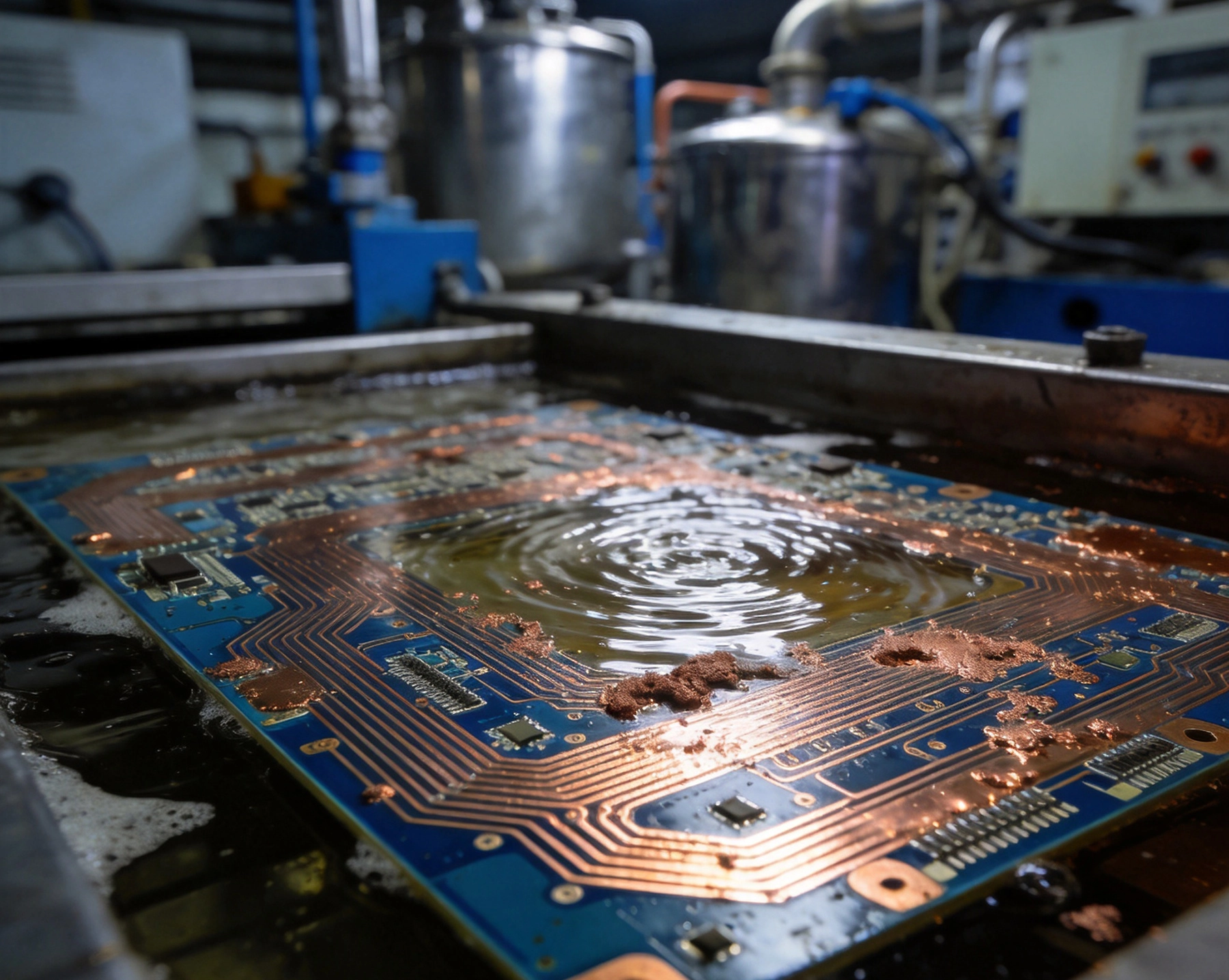
Heavy copper PCBs serve critical applications in Power Electronics, automotive systems, industrial equipment, and renewable energy systems. These boards handle high currents, require superior Thermal Management, and must maintain electrical integrity under demanding operating conditions. Common applications include power converters, motor drives, battery management systems, and high-current distribution boards where copper traces can reach 10 oz (350 μm) or more in thickness. The thick copper layers provide lower resistance, better Heat Dissipation, and increased mechanical strength, making them ideal for power-hungry applications.
The transition to heavy copper introduces several manufacturing complexities. The increased copper mass significantly affects etch rates, undercut characteristics, and dimensional control. Standard etching parameters optimized for 1 oz copper often fail when applied to heavy copper, resulting in either incomplete etching or excessive undercut, both compromising board functionality. Manufacturers must adapt their processes to accommodate these physical differences while maintaining tight tolerance requirements specified by industry standards such as IPC-6012 and IPC-2221.
The most significant tolerance challenge in heavy copper etching relates to the etch factor—the relationship between horizontal undercut and vertical copper removal. With standard copper thicknesses, etch factors typically range from 1:1 to 1.5:1, meaning for every unit of vertical copper removed, the horizontal undercut remains relatively controlled. However, heavy copper dramatically shifts this ratio. As etchant penetrates deeper into thicker copper, the lateral etching increases disproportionately, leading to trace width variations and spacing reductions that can exceed allowable tolerances.
Trace width control becomes particularly problematic with heavy copper. For example, a 10 mil (0.254 mm) wide trace on 4 oz (140 μm) copper might require design compensation of 2-3 mils to account for undercut, whereas the same trace on 1 oz copper might need only 0.5-1 mil compensation. This difference stems from the longer etch duration required for heavy copper, which allows etchant more time to attack sidewalls laterally. Additionally, the increased copper mass creates more heat generation during the etching process, potentially leading to temperature variations that further affect etch rates and uniformity across the panel.
Another critical tolerance issue involves maintaining uniform copper removal across the entire panel area. Heavy copper etching typically requires longer processing times, increasing the likelihood of non-uniform etching due to fresh etchant concentration gradients, temperature variations, and agitation inconsistencies. Non-uniform etching can result in over-etched areas where traces become too narrow or under-etched areas where unwanted copper remains, both creating yield-reducing defects. The challenge compounds with panel size, as larger panels exacerbate these uniformity problems.
The chemical composition of the etching solution significantly impacts heavy copper etching performance. Traditional ferric chloride (FeCl3) etchants, while effective for standard copper thicknesses, struggle with heavy copper due to their limited capacity and potential for excessive undercut at the extended processing times required. Alternative etchants like cupric chloride (CuCl2) and ammonium persulfate ((NH4)2S2O8) offer different characteristics that may better suit heavy copper applications, each with distinct advantages regarding etch rate control, undercut characteristics, and solution life.
Etchant concentration management becomes increasingly critical with heavy copper processing. As copper dissolves into the solution, the effective etching power decreases, requiring careful monitoring and replenishment to maintain consistent etch rates throughout the production run. This challenge intensifies with heavy copper due to the larger volume of copper removed per panel. Manufacturers implementing heavy copper capabilities must establish robust concentration control systems with frequent analysis and automated replenishment capabilities to prevent etch rate variations that could compromise tolerances.
Temperature control represents another crucial variable. Higher etchant temperatures generally increase etch rates but also accelerate undercut, creating a delicate balance that requires precise control. Heavy copper etching generates significant heat due to the exothermic nature of the copper dissolution reaction, potentially raising etchant temperature beyond setpoints during processing. Effective temperature regulation systems with adequate cooling capacity become essential to maintain stable etching conditions throughout the extended processing times required for heavy copper removal.
Addressing heavy copper etching challenges requires a multi-faceted approach combining process optimization, equipment selection, and Design For Manufacturing (Dfm) principles. One effective solution involves implementing multi-stage etching processes where heavy copper boards undergo initial rough etching followed by precision etching passes. The rough etch rapidly removes the bulk copper thickness while the precision etch fine-tunes the final dimensions with tighter control. This approach reduces overall processing time while improving tolerance control compared to single-pass etching.
Spray etching systems with optimized nozzle configurations and controlled pressure settings provide superior performance for heavy copper applications compared to dip or tank etching methods. The directed spray action enhances etchant delivery to deep copper layers while simultaneously removing dissolved copper from the immediate etching zone, maintaining fresh chemical activity at the copper surface. Variable pressure systems that start with higher pressure during the bulk copper removal phase and reduce pressure during the final precision etch help minimize undercut while maintaining adequate etch rates.
Real-time monitoring systems employing optical inspection, copper thickness measurement, or conductivity sensing enable process control adjustments during etching rather than after completion. These systems can detect developing non-uniformities or approaching tolerance limits, allowing operators or automated control systems to make immediate corrections to spray patterns, temperature, or etchant flow. Such closed-loop control systems significantly improve yield and consistency for heavy copper production, reducing the need for scrap and rework.
Successful heavy copper PCB Fabrication begins with design considerations that account for etching limitations. Designers should implement appropriate design rules including increased minimum trace widths, larger spacing requirements, and appropriate copper thickness specifications based on current carrying needs rather than arbitrary over-design. For example, calculating the exact copper thickness required for a given current using IPC-2221 formulas helps avoid unnecessarily thick copper that complicates etching without providing proportional benefits.
Design compensation plays a crucial role in achieving final dimensions within tolerance. Heavy copper boards require more aggressive design compensation than standard PCBs, with trace widths and spacings intentionally oversized to account for undercut during etching. The compensation amount depends on multiple factors including copper thickness, etchant type, processing parameters, and equipment characteristics. Collaboration between PCB designers and manufacturers helps establish appropriate compensation factors based on actual process capabilities rather than generic guidelines.
Pad size and shape modifications help address heavy copper etching challenges, particularly for through-hole components and surface mount lands. Increased pad sizes accommodate undercut while ensuring adequate land area for reliable solder connections. Tear-drop pad shapes or reinforced connections between pads and traces help maintain structural integrity when trace widths narrow due to etching. Additionally, providing generous spacing between features reduces the risk of bridging defects caused by non-uniform etching or over-etching in tight areas.
Implementing comprehensive process control systems represents the foundation for successful heavy copper etching operations. Statistical process control (SPC) methodologies track critical parameters including etch rate, undercut dimensions, trace width consistency, and copper thickness uniformity. Control charts identify trends indicating process drift before tolerances are exceeded, enabling preventive adjustments. Establishing specification limits that are more restrictive than final board tolerances creates buffer zones that accommodate normal process variation while ensuring final product compliance.
Regular process validation through test coupons and qualification panels provides essential data for ongoing process capability assessment. Heavy copper production should include process control coupons on every production panel, featuring trace widths, spacings, and copper thicknesses representative of the actual board design. These coupons enable post-etch measurement verification without damaging functional circuits, providing early warning of process deviations before they affect production yield.
Inspection and measurement capabilities specifically adapted for heavy copper boards help ensure consistent quality. Advanced optical inspection systems with appropriate lighting and resolution detect undercut, trace width variations, and other dimensional anomalies. Destructive testing through cross-section analysis validates internal copper removal characteristics and verifies that etching penetrated through the full copper thickness without excessive undercut. Regular equipment calibration and maintenance of inspection systems ensure measurement accuracy essential for maintaining tight tolerances.
Advanced etching technologies continue to evolve, offering improved solutions for heavy copper manufacturing challenges. Laser-assisted etching combines chemical etching with laser ablation to enhance precision and control. The laser selectively removes thin layers of copper before chemical etching, reducing the total chemical etching time and associated undercut. This hybrid approach particularly benefits applications requiring extremely tight tolerances on very heavy copper boards where traditional methods struggle to maintain dimensional accuracy.
Alternative subtractive manufacturing methods like plasma etching provide chemical-free copper removal capabilities. Plasma etching systems utilize reactive ion etching (RIE) or inductively coupled plasma (ICP) to remove copper through physical and chemical reactions in a vacuum environment. While currently expensive and limited in panel size compared to wet chemical etching, plasma systems offer superior control over undercut and dimensional accuracy, making them attractive for high-value, high-reliability applications where performance justifies the cost.
Additive manufacturing approaches complement subtractive etching methods for heavy copper applications. Semi-additive processes build copper traces through electroplating onto a thin seed layer rather than etching away unwanted copper. This method eliminates undercut concerns entirely since copper is only added where needed. While semi-additive processes historically faced limitations with very thick copper, recent advances enable copper thicknesses up to 6 oz (210 μm) with excellent dimensional control, making them increasingly viable for heavy copper applications previously dominated by subtractive etching.
Heavy Copper Pcb etching presents significant but surmountable challenges requiring specialized knowledge, equipment, and process controls. Understanding the fundamental tolerance issues related to etch factor, trace width control, and uniformity provides the foundation for developing effective solutions. Implementing multi-stage etching processes, advanced spray systems, real-time monitoring, and comprehensive Dfm practices enables manufacturers to achieve consistent quality within tight tolerance requirements.
Success in heavy copper etching demands collaboration across the entire Pcb Fabrication ecosystem. Designers must understand manufacturing limitations and implement appropriate design rules and compensation. Manufacturers must invest in appropriate equipment, develop robust process controls, and maintain rigorous Quality Assurance systems. Material suppliers must provide etchants, photoresists, and other materials specifically optimized for heavy copper applications. When all stakeholders work together with a shared understanding of the unique challenges and requirements, heavy copper PCBs can be manufactured consistently and reliably to meet the demanding needs of modern Power Electronics applications.
As technology continues advancing, new solutions will further improve heavy copper etching capabilities. Laser-assisted systems, plasma etching, and additive processes represent the cutting edge of heavy copper manufacturing technology. However, the fundamental principles of process control, Design Optimization, and Quality Assurance remain constant. By mastering these principles while embracing emerging technologies, PCB fabricators can successfully navigate the challenges of heavy copper etching and deliver high-performance boards that meet increasingly demanding application requirements.

China vs. Local PCB Suppliers: Analyzing Cost, Quality, and Lead TimeJuly/22/2026
Understanding Surface Finishes: ENIG, HASL, OSP, and Immersion SilverJuly/21/2026

PCB Fabrication China: A Complete Guide for Global BuyersMay/18/2026
Laser Drilling vs. Mechanical Drilling: Precision in HDI ManufacturingJuly/07/2026
Preparing Your Gerber Files for a Smooth China PCB Fabrication ProcessSeptember/18/2026
PCB Prototype Manufacturing in China: Complete GuideMay/18/2026

Sourcing Metal Core PCBs for Automotive LED HeadlightsJuly/25/2026

Wearable Health Monitors: The Importance of Biocompatible Flex PCBsSeptember/02/2026