Open Nav

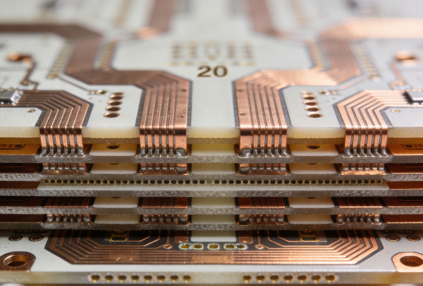
How to Design High-Layer Count PCBs (20+ Layers) for Complex ElectronicsSeptember/08/2026Designing a printed circuit board with 20 or more layers is not simply a matter of stacking more copper onto a familiar structure. As layer count climbs past the ten-layer mark and into the territory of 20, 24, 32, or even 64 layers, every design decision carries compounded consequences. Signal in...
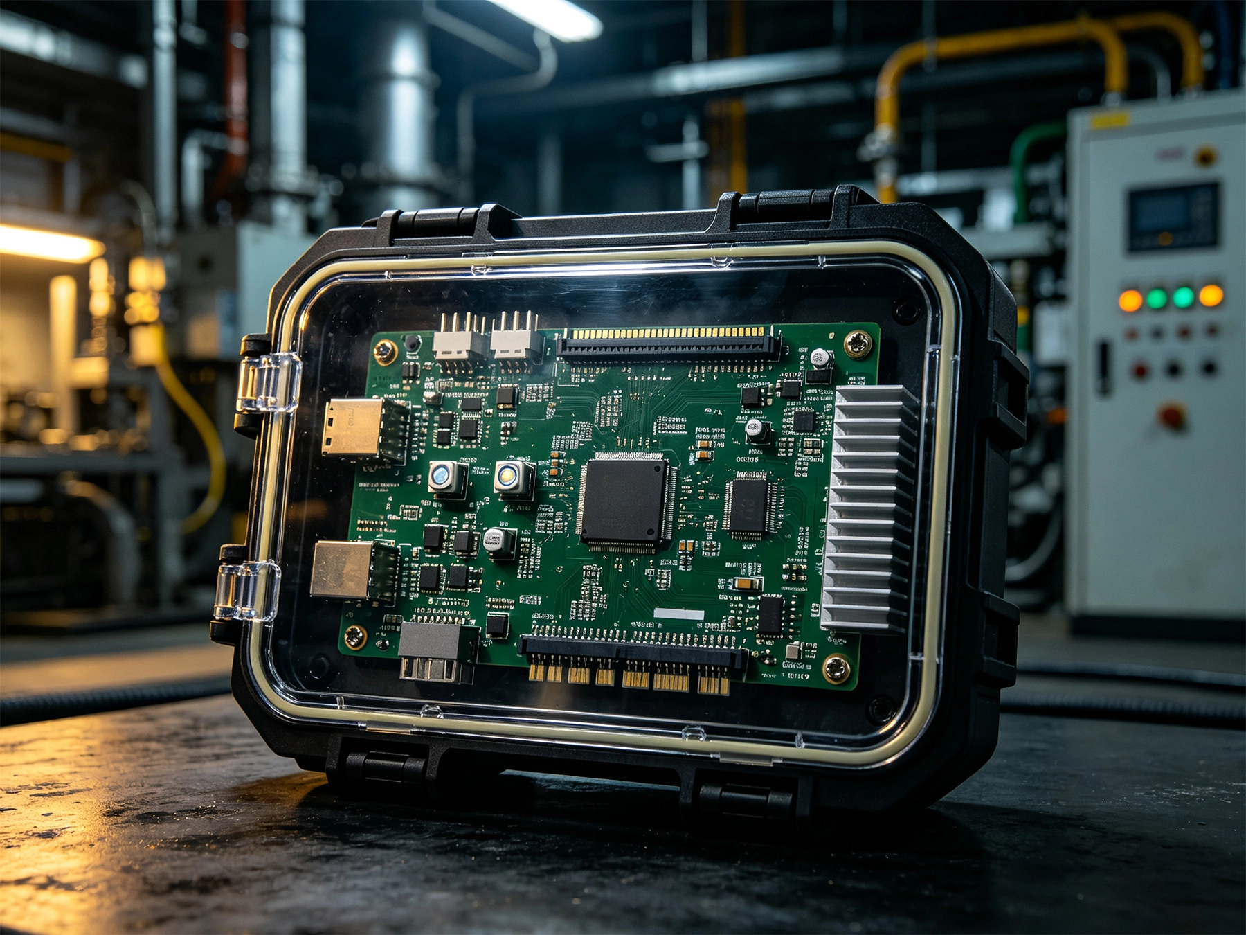
Durability Requirements for Industrial IoT PCBs: Ensuring Reliability in Harsh EnvironmentsSeptember/03/2026Industrial IoT (Internet of Things) devices operate in environments that would quickly destroy standard consumer electronics. From factory floors exposed to dust and chemicals to outdoor installations subjected to extreme temperatures, these devices must maintain reliable performance year after ye...
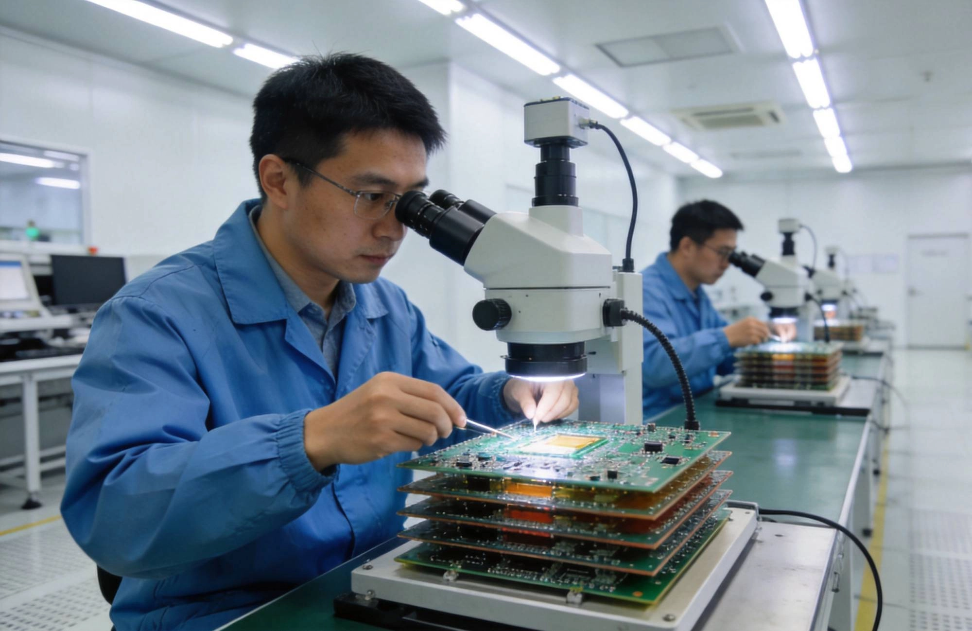
How We Ensure Quality Control in Multilayer PCB LaminationAugust/08/2026When a smartphone fails to boot or a medical device shuts down unexpectedly, the root cause often traces back to a single manufacturing stage: multilayer PCB lamination. This critical process bonds multiple layers of conductive and insulating materials under precise heat and pressure conditions. A...
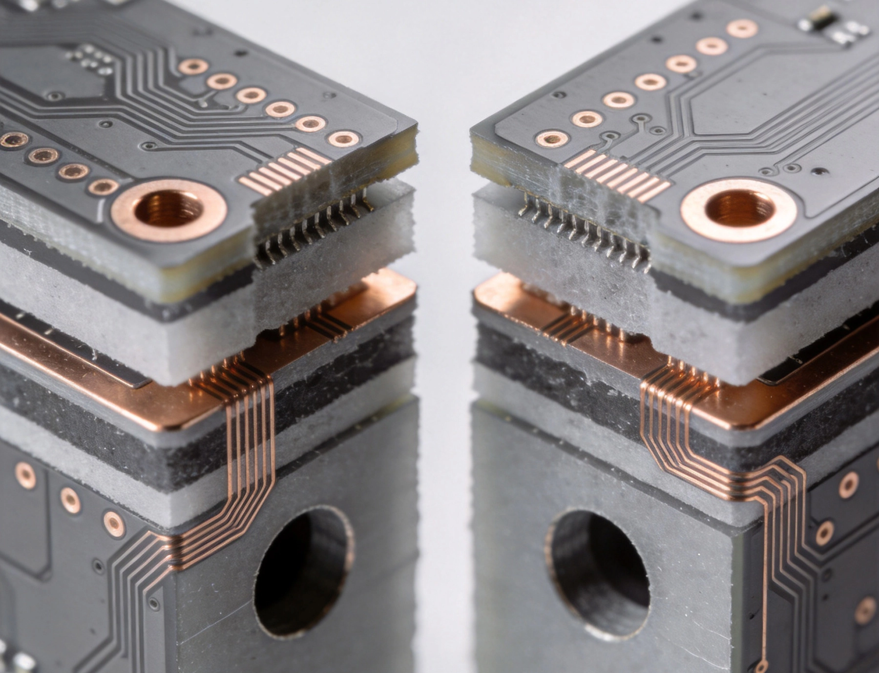
Microvias vs. Through-Holes: Choosing the Right Tech for Your Multilayer BoardAugust/06/2026Modern electronics continue shrinking while demanding more functionality, forcing PCB designers to make critical decisions about interconnect technology. At the heart of this challenge lies a fundamental choice: microvias or through-holes. Each technology offers distinct advantages, and selecting ...
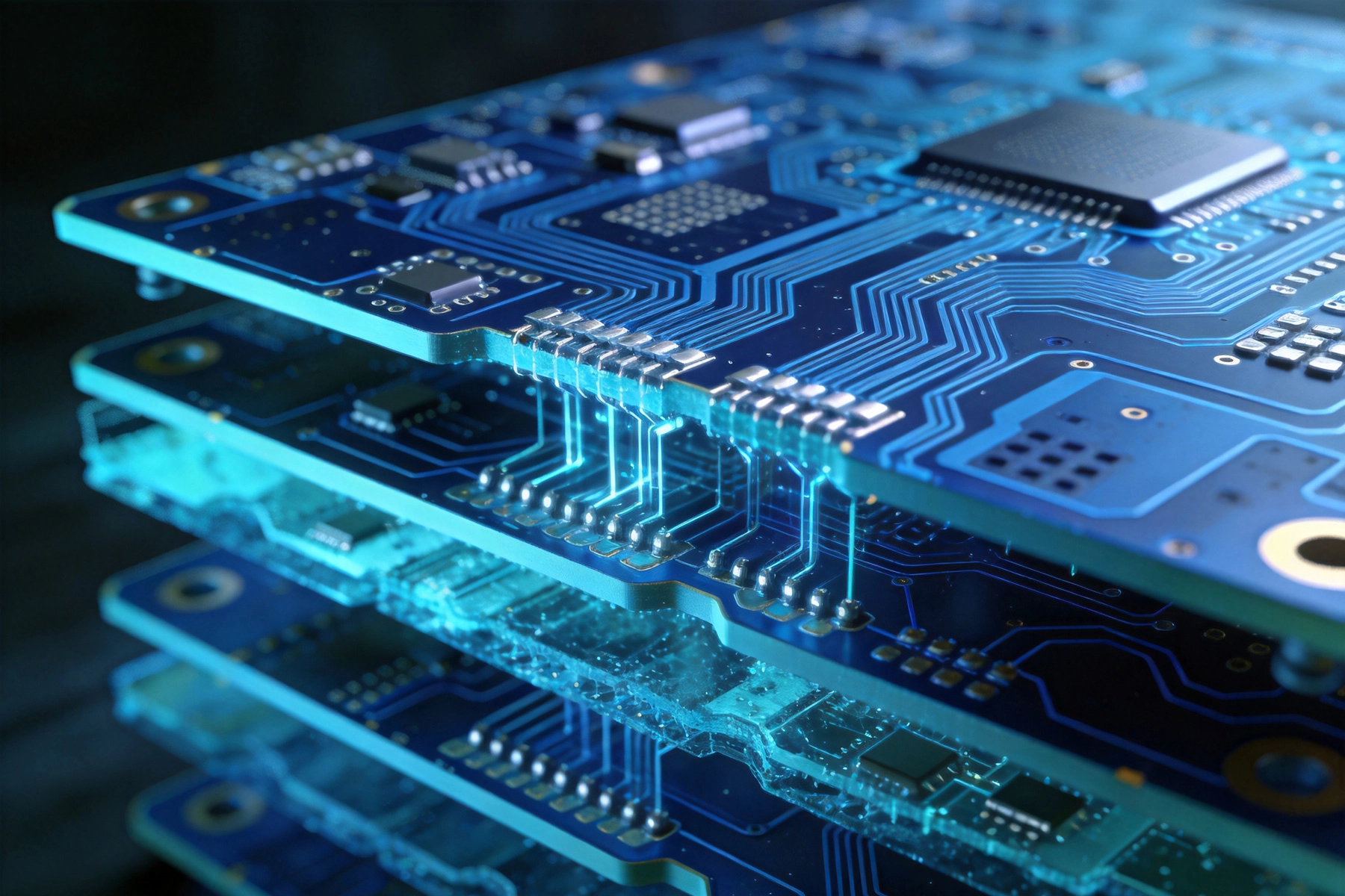
Understanding HDI PCB Stack-ups: Best Practices for High-Density DesignsJuly/18/2026High-Density Interconnect (HDI) printed circuit boards have become the backbone of modern electronics, enabling the compact, high-performance devices we rely on daily. From smartphones to medical implants, HDI technology allows designers to pack more functionality into smaller form factors while m...
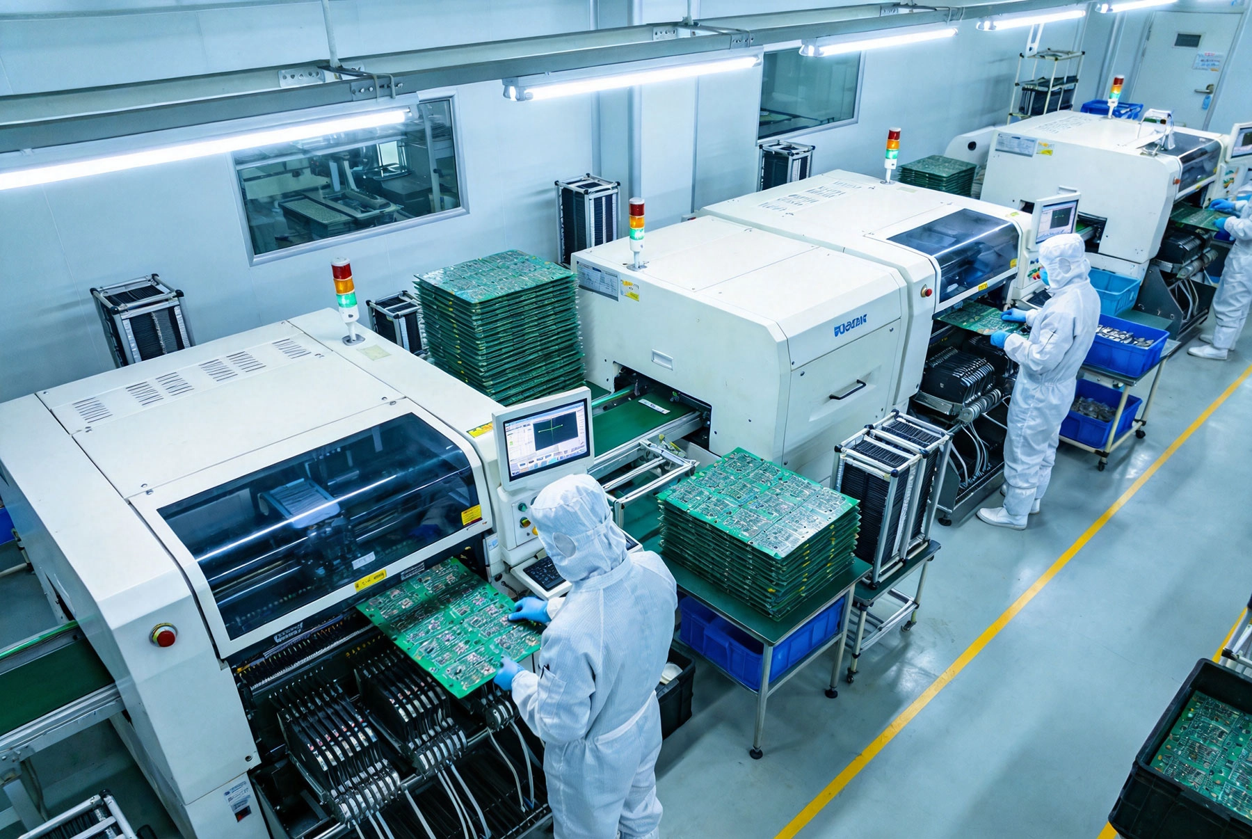
Behind the Scenes: A Tour of Our State-of-the-Art PCB Factory in ChinaMay/19/2026China has long been the world's manufacturing powerhouse, and nowhere is this more evident than in the production of printed circuit boards. Every smartphone, laptop, medical device, and automotive control system that you use likely contains PCBs that were designed, engineered, and manufactured wi...
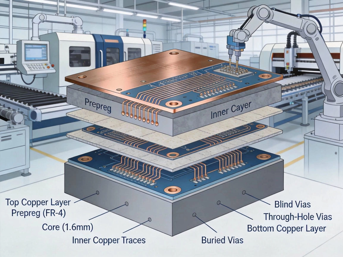
What Are Multilayer PCBs? A Complete Guide from ChinaMay/18/2026Multilayer PCBs represent the advanced standard in modern electronics manufacturing, enabling complex devices we use daily. From smartphones to servers, these sophisticated circuit boards pack exceptional functionality into compact spaces. As a China PCB manufacturer with 15+ years producing 120M+...