Open Nav

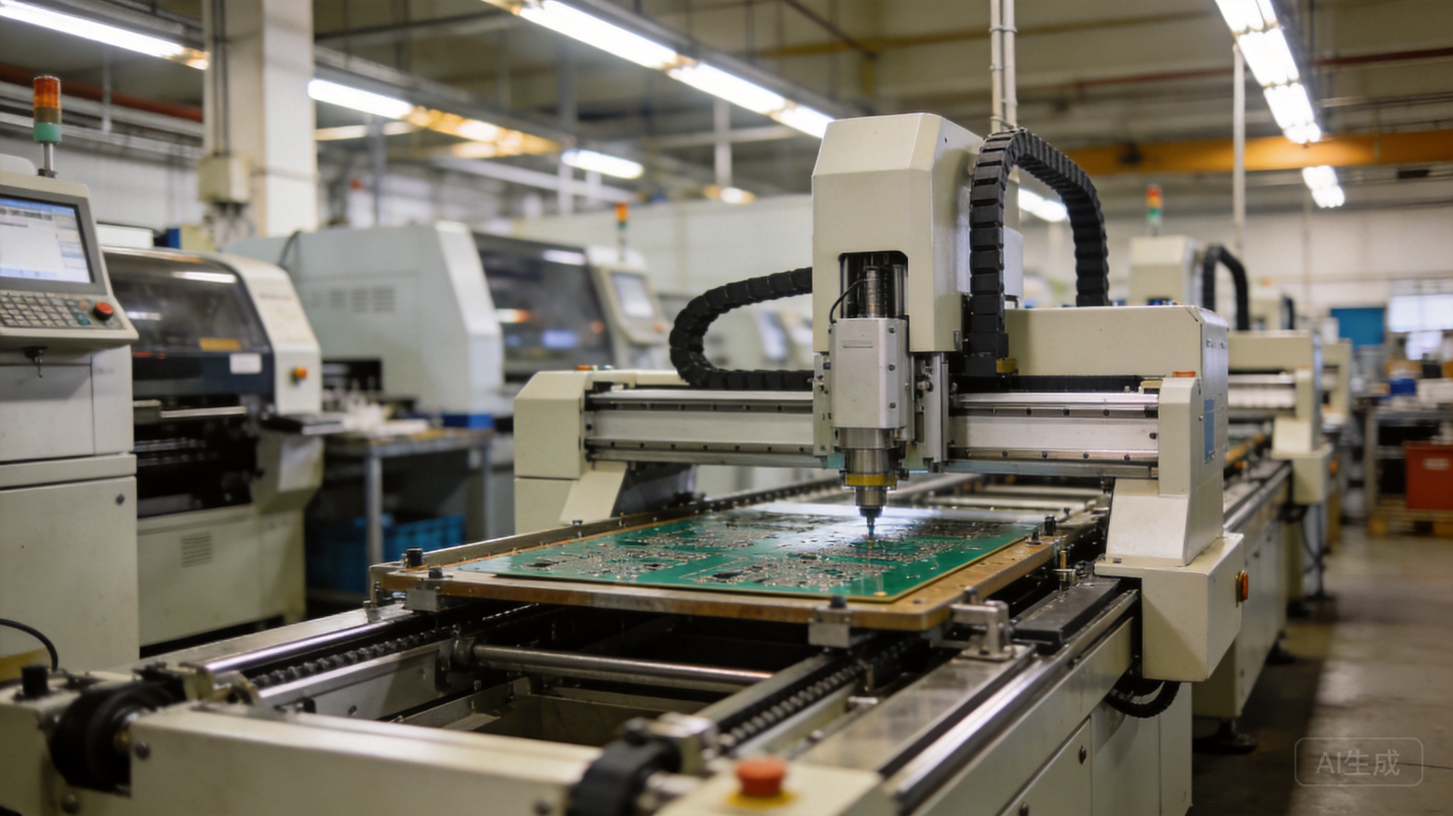
When ordering PCB prototypes for your electronics projects, understanding Pcb Prototype pricing models becomes crucial for budget management. Most engineers and procurement specialists encounter sticker shock when they see setup fees and panelization costs added to their first quotes. This comprehensive guide breaks down these pricing structures, explaining how panelization and setup fees work, and provides practical strategies to optimize your PCB Fabrication costs while maintaining quality standards.
Setup fees represent the fixed costs that PCB manufacturers incur when preparing your design for production, regardless of order quantity. These fees cover the initial engineering work, tooling preparation, and administrative processes required to get your Pcb Prototype from digital files to physical boards. Understanding these costs helps you make informed decisions about when to consolidate orders and how to structure your prototype development timeline.
The setup fee typically includes several components that may vary between manufacturers but generally encompass engineering review, data preparation, phototool creation, and machine programming. When you submit your Gerber files, engineers must verify that they meet manufacturing capabilities, check for design rule violations, and ensure all necessary layers are present and properly formatted. This engineering review time adds to the setup cost but helps prevent expensive Manufacturing Errors that could render your prototypes unusable.
Phototool creation involves producing the physical or digital masks used to transfer your circuit pattern onto copper-clad laminates. For standard double-sided boards, this means creating two phototools, while multilayer boards require multiple sets of phototools corresponding to each copper layer. The precision required for these tools means they cannot be reused between different designs, making this a true setup cost specific to your PCB prototype.
Engineering and data preparation fees cover the time spent reviewing your design files and converting them into manufacturing-ready formats. This includes checking layer alignment, verifying drill files, ensuring proper solder mask and silkscreen layers, and confirming that your design matches the manufacturer's capabilities. While this might seem like unnecessary overhead, experienced engineers often catch design flaws that would otherwise cause production delays or defective boards.
Phototool and tooling costs represent the physical materials and equipment time needed to create production masks. Modern PCB Fabrication may use laser direct imaging systems instead of traditional phototools, but these systems still require setup time and calibration specific to your design. The complexity of your design, including the number of layers and minimum feature sizes, directly impacts these tooling costs.
Machine programming and setup fees account for the time spent configuring CNC drilling machines, routing equipment, and other production tools for your specific design. Each board size, layer count, and hole pattern requires different machine parameters, and skilled technicians must program and verify these settings before production can begin. This programming work cannot be shared between different designs, making it a legitimate setup cost.
Panelization refers to the process of arranging multiple individual PCB units onto a single larger panel for simultaneous manufacturing. This technique fundamentally changes PCB prototype pricing models by allowing manufacturers to spread fixed costs across multiple boards. For small to medium-sized prototypes, panelization can significantly reduce per-unit costs while maintaining the same quality and turnaround times as single-board production.
The economics of panelization work on a simple principle: manufacturing one large panel requires approximately the same setup time, machine programming, and tooling costs as manufacturing a single small board. By fitting multiple copies of your design onto one panel, you effectively divide these fixed costs across all the units on that panel. This is particularly advantageous for prototype runs where you need multiple identical boards for testing, development teams, or early customer evaluation.
However, panelization isn't always the optimal choice for every PCB prototype project. Very large boards or designs with complex shapes may not panelize efficiently, potentially wasting material and increasing costs without providing meaningful savings. Similarly, if you only need one or two prototype boards, the material waste from panelization might offset any setup fee savings. Understanding your specific requirements helps determine whether panelization makes economic sense for your project.
Standard rectangular panelization arranges identical PCB copies in a grid pattern on a standard manufacturing panel size, typically 18x24 inches or 12x18 inches depending on the manufacturer. This approach maximizes board yield when your design has regular dimensions that fit cleanly into the panel without excessive waste. Engineers can often optimize panel layouts by rotating boards or adjusting spacing to fit more units per panel, directly impacting the per-unit cost of your PCB prototype.
Stepped or staggered panelization involves offsetting alternating rows of boards to minimize material waste when dealing with boards that don't fit cleanly into a rectangular grid. This technique can sometimes squeeze additional units onto a panel, particularly for boards with odd aspect ratios. However, stepped panels may require additional routing considerations and can complicate assembly processes, so manufacturers may charge extra for this service.
Multi-design panelization allows you to place different PCB designs onto the same manufacturing panel, which can dramatically reduce setup fees when you need multiple prototype boards for a single project. Instead of paying separate setup fees for each design, you pay one setup fee for the entire panel containing all your designs. This approach works best when all designs share similar specifications (layer count, material type, surface finish) and when the manufacturer offers this service, which not all do.
V-score panelization creates shallow grooves between individual boards on the panel, allowing them to be easily separated after assembly by applying pressure along these score lines. This method provides clean, consistent breaks and eliminates the need for routing tabs, which can leave rough edges. However, V-scoring requires boards to be arranged in straight rows with consistent spacing, which may reduce panel utilization for some designs.
The relationship between setup fees and panelization creates interesting dynamics in PCB prototype pricing models that savvy engineers can leverage to their advantage. When you choose to panelize your design, you're making a strategic decision to trade some flexibility for cost efficiency. The key is understanding how these pricing elements interact and when each approach provides better value for your specific project requirements.
For a single PCB prototype ordered without panelization, you pay the full setup fee for one board. If you order the same design panelized to produce ten boards, you still pay only one setup fee, but now that cost is divided across ten units instead of one. This dramatically reduces the per-unit setup cost from 100% to just 10% per board. However, you're now committed to ordering ten boards even if you only need a few for initial testing, which represents a different kind of cost—potential waste of materials and money if the design needs significant revisions.
Many manufacturers offer tiered pricing where the setup fee decreases with larger order quantities, even without panelization. In these cases, the decision becomes more nuanced: you might find that ordering 5-10 single boards provides similar per-unit costs to a panelized order of 20 boards, without requiring you to purchase more prototypes than you actually need. Understanding your manufacturer's specific pricing structure becomes essential for making the most economical choice.
Some manufacturers waive setup fees entirely for larger orders, typically 100+ boards, recognizing that the volume makes these fixed costs negligible. For projects moving from prototype to production, this creates a natural transition point where panelization becomes less relevant and per-unit pricing dominates the cost structure. Smart project planning can take advantage of these inflection points by timing your prototype orders to align with volume discount thresholds.
When evaluating PCB prototype pricing models, it's essential to look beyond the initial quote and consider the Total Cost Of Ownership for your prototyping needs. A lower per-unit price from panelization might represent poor value if you end up with excess boards that you can't use. Conversely, paying higher per-unit costs for single boards might prove economical if it allows you to test design iterations more quickly and move to production faster.
Consider the cost of design revisions when planning your prototype strategy. If you anticipate multiple design iterations based on initial testing, ordering smaller quantities of single boards might actually save money overall, even with higher per-unit costs. Each design change would require new setup fees, but you wouldn't be stuck with large quantities of obsolete designs from panelized orders. This iterative approach often proves more cost-effective for early-stage development where design uncertainty remains high.
Assembly costs also factor into the true economics of panelization. If you plan to have your PCB prototypes assembled, most assemblers charge per board rather than per panel, potentially negating some of the fabrication savings from panelization. However, some assemblers offer volume discounts that make panelized boards more economical. Coordinate your fabrication and assembly planning to ensure you're optimizing the total cost, not just individual components.
Armed with understanding of PCB prototype pricing models, you can implement several strategies to reduce your prototyping costs without sacrificing quality or functionality. These approaches range from simple design adjustments to strategic ordering practices that leverage manufacturer capabilities and pricing structures. The goal is to minimize expenses while still achieving your development objectives on schedule.
Design Optimization represents the most fundamental opportunity for Cost Reduction in Pcb Prototyping. By adhering to standard manufacturing capabilities rather than pushing for tighter tolerances or unusual specifications, you can often qualify for standard pricing tiers rather than premium or special processing charges. This includes using standard layer counts, trace widths, and hole sizes that align with manufacturer's base capabilities rather than requesting exotic features that trigger additional fees.
Consolidating orders provides another effective cost-saving strategy. If you have multiple PCB designs needed for the same project or timeframe, combining them into a single order can reduce total setup fees. Some manufacturers offer significant discounts for multi-design orders or may waive setup fees for additional designs beyond the first. This approach works particularly well when all designs share similar specifications and can be manufactured using the same materials and processes.
Timing your orders strategically can yield substantial savings. Many manufacturers offer periodic promotions, especially during slower business periods, which may include reduced setup fees or free panelization. Planning your prototyping schedule to align with these promotions can reduce costs without affecting your development timeline. Additionally, some manufacturers offer better pricing for orders with longer lead times, allowing you to trade time for money if your schedule permits.
Building a relationship with your PCB manufacturer can lead to better pricing over time, especially for regular prototyping needs. Manufacturers value consistent business and may offer discounted rates or waived setup fees for customers who place regular orders. This relationship-based pricing reflects the reduced administrative overhead and more predictable production planning that comes with repeat customers.
Don't hesitate to negotiate pricing, especially for larger or recurring orders. Many PCB manufacturers have some flexibility in their pricing structure, particularly for customers who bring significant volume or who represent potential long-term business. Being transparent about your expected volume and timeline can sometimes unlock better terms than those initially quoted. However, remember that manufacturers have legitimate costs to cover, so negotiations should be reasonable and focused on finding mutual benefit.
Consider seeking quotes from multiple manufacturers to understand market pricing for your specific requirements. However, be cautious about simply choosing the lowest quote without considering other factors like quality, reliability, and customer service. The cheapest option may prove more expensive in the long run if it results in delays, quality issues, or poor communication that slows your development process. Look for manufacturers who offer competitive pricing while also demonstrating technical expertise and responsive customer support.
While the basic principles of PCB prototype pricing models apply to most projects, complex designs introduce additional cost factors that deserve special consideration. High-density Interconnect (HDI) boards, flexible circuits, and designs requiring specialized materials or processes often follow different pricing structures that reflect their increased manufacturing complexity. Understanding these special cases helps you budget accurately and make informed design decisions.
HDI PCBs typically command higher setup fees due to the specialized processes required for their fabrication, including Laser Drilling for Microvias and Sequential Lamination for multiple build-up layers. These advanced processes require expensive equipment and greater technical expertise, both of which contribute to higher costs. However, the benefits of Hdi Technology—smaller form factors, better electrical performance, and increased functionality—often justify these additional costs for advanced electronic products.
Flexible and rigid-flex PCBs introduce unique panelization challenges that affect pricing strategies. The flexible nature of these circuits requires specialized handling during manufacturing and often precludes standard panelization approaches used for rigid boards. Many manufacturers charge premium pricing for flexible circuits to account for these process differences and the higher material costs associated with flexible substrates. When prototyping flexible circuits, focus on optimizing your design for the manufacturer's specific Flexible Pcb capabilities rather than trying to apply rigid board cost-reduction strategies.
Boards requiring exotic materials—such as high-frequency laminates, metal-core substrates for Thermal Management, or specialized ceramic materials for extreme environments—typically involve higher material costs that may dwarf setup fee considerations. In these cases, optimizing your design to minimize material usage or selecting the most cost-effective material that still meets your technical requirements becomes the primary cost-reduction strategy. Setup fees still matter, but they represent a smaller portion of the total cost compared to standard FR4 boards.
The PCB industry continues evolving, and pricing models adapt alongside technological advances and market dynamics. Understanding emerging trends in PCB prototype pricing helps you anticipate future costs and make strategic decisions about your prototyping processes. Several trends currently shaping the industry have direct implications for how prototype pricing will work in the coming years.
Automation in Pcb Fabrication is reducing manual setup times and labor costs, which should gradually decrease setup fees for standard designs. Advanced manufacturing equipment with automated loading, alignment, and quality checking reduces the technician time required for each job. However, this automation also requires significant capital investment, which manufacturers must recoup through their pricing structures. The net effect may be lower setup fees for standard designs but potentially higher minimum order quantities as manufacturers seek to maximize equipment utilization.
Digital manufacturing technologies, including direct imaging systems that eliminate traditional phototools, are changing the cost structure of Pcb Prototyping. These technologies reduce some traditional setup costs but introduce new equipment and maintenance expenses. The pricing impact varies by manufacturer and technology implementation, with some passing savings to customers while others use the efficiency improvements to support lower minimum order quantities rather than reducing per-unit prices.
The globalization of Pcb Manufacturing continues to influence pricing models, with increased competition from Asian manufacturers putting downward pressure on prototype costs. However, this competition also creates challenges in communication, Quality Control, and Intellectual Property Protection that may offset pure cost savings for some companies. Smart procurement strategies balance cost considerations with quality, reliability, and strategic factors to find the optimal manufacturing partners for specific project needs.
Q: Are setup fees refundable if I need to make design changes?
A: Generally, setup fees are non-refundable because they represent actual costs incurred by the manufacturer in preparing your design for production. If you need to make design changes, you'll typically need to pay a new setup fee for the revised design. However, some manufacturers offer partial credits or discounts for revisions when the changes are minimal or when they result from manufacturing issues rather than design errors.
Q: Can I avoid setup fees by ordering larger quantities?
A: Many manufacturers do waive or reduce setup fees for larger order quantities, though the thresholds vary significantly between suppliers. Some eliminate setup fees entirely for orders of 100+ boards, while others offer tiered pricing where the per-unit setup cost decreases with quantity. When planning your prototype orders, consider whether you can consolidate multiple small orders into one larger order to qualify for these quantity-based discounts.
Q: How do I know if panelization makes sense for my project?
A: Panelization typically makes economic sense when you need multiple identical boards and your design panels efficiently without excessive material waste. Calculate the per-unit cost both with and without panelization, considering your actual quantity needs. If panelization reduces per-unit costs by more than the value of any excess boards you won't use, it's probably the better choice. For very small quantities or designs that don't panelize efficiently, single-board pricing often proves more economical despite higher per-unit costs.
Q: Do all manufacturers charge setup fees the same way?
A: No, PCB manufacturers use various pricing models, and setup fee structures can differ significantly. Some charge flat setup fees regardless of design complexity, while others scale setup costs based on layer count, board size, or technical difficulty. Some bundle setup fees into per-unit pricing, while others itemize them separately. Always request detailed quotes that break down all costs so you can make accurate comparisons between suppliers.
Q: Can I reduce setup fees by providing production-ready files?
A: While providing clean, correctly formatted files can prevent additional engineering charges, it rarely eliminates setup fees entirely because these fees cover more than just file preparation. However, thorough design review before submitting files can prevent costly revisions and additional setup fees for corrected designs. Some manufacturers offer reduced engineering fees for designs that pass automated DRC checks without issues, so investing time in design verification before submission can save money.
Understanding PCB prototype pricing models, particularly the roles of setup fees and panelization, empowers you to make smarter decisions about your Electronics Development projects. By recognizing how these pricing elements work and interact, you can optimize your prototyping strategy to balance cost efficiency with development speed and quality requirements. The key is approaching prototyping as a strategic process rather than simply ordering the cheapest available option.
Successful prototyping requires balancing multiple factors: cost, quality, speed, and flexibility. Setup fees and panelization represent tools in your optimization toolkit, not immutable cost structures. By understanding when to leverage panelization's volume advantages and when to prioritize single-board flexibility, you can develop a prototyping approach that serves your specific project needs while keeping costs under control.
As you plan your next PCB prototype project, take time to analyze your quantity needs, design complexity, and timeline constraints. Use this understanding to evaluate different pricing options and work collaboratively with your manufacturer to find the most cost-effective approach. With strategic planning and informed decision-making, you can stretch your prototyping budget further while still achieving your development objectives on schedule.
Remember that the cheapest option isn't always the most economical when you consider the total cost of development, including potential delays, quality issues, and wasted materials from poor planning. Focus on optimizing the overall prototyping process rather than minimizing individual line items, and you'll achieve better results for your Electronics Development projects.
PCB Prototype Manufacturing in China: Complete GuideMay/18/2026

10 Questions to Ask Your Potential PCB Prototype Manufacturer in ChinaJuly/07/2026

How We Handle Intellectual Property Protection for Overseas ClientsOctober/19/2026
Evaluating a China Multilayer PCB Manufacturer: Certifications and CapabilitiesSeptember/11/2026
IoT Devices and the Demand for Compact, Low-Cost PCB PrototypesJuly/31/2026
Bridging the Gap: Moving from PCB Prototype to Mass ProductionOctober/09/2026
Designing for SMT: Pad Sizes, Spacing, and OrientationJuly/12/2026

The Future of PCB Manufacturing in China: Trends for 2026 and BeyondMay/19/2026