
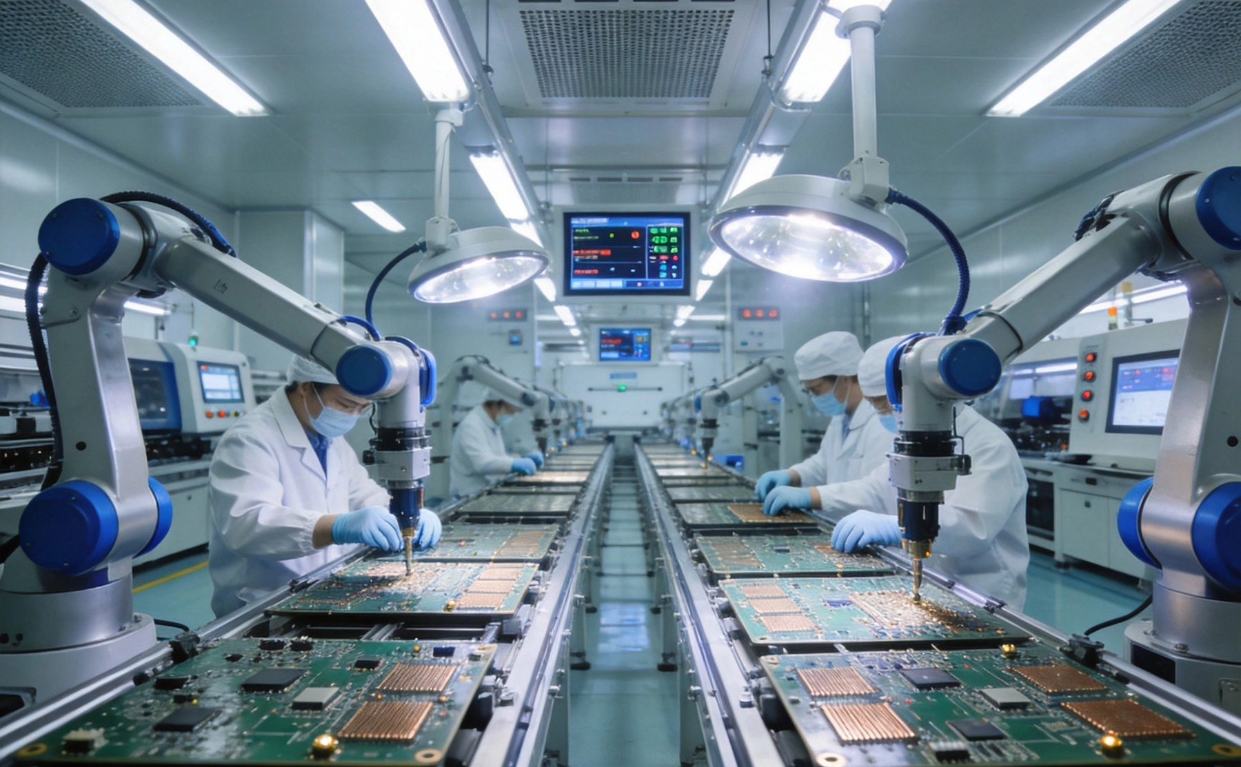
If you've ever wondered how those impossibly dense printed circuit boards inside your smartphone or tablet come to life, you're not alone. The HDI PCB manufacturing process is one of the most sophisticated operations in modern electronics productio...
https://www.china-pcbmanufacturer.com/china-hdi-pcb-manufacturer/hdi-pcb-manufacturing-process-step-by-step-explanation/
Modern electronics are locked in an ongoing battle for space. Every new generation of smartphone, wearable, medical implant, and automotive module demands more functionality packed into a smaller footprint. Meeting that demand starts at the board l...
https://www.china-pcbmanufacturer.com/china-rigid-flex-pcb-manufacturer/blind-and-buried-vias-enhancing-density-in-hdi-pcbs/