Open Nav

Modern electronics are locked in an ongoing battle for space. Every new generation of smartphone, wearable, medical implant, and automotive module demands more functionality packed into a smaller footprint. Meeting that demand starts at the board level — and one of the most effective ways to increase circuit density without enlarging the PCB is through the strategic use of blind and buried vias.
If you have worked with multilayer PCBs for any length of time, you have probably encountered these terms. But understanding the practical difference between a Blind Via and a Buried Via — and knowing when to use each — can make the difference between a board that barely fits and one that performs reliably under thermal and mechanical stress.
This article breaks down what blind and buried vias are, how they are fabricated, what design rules to follow, and where they show up in real products.
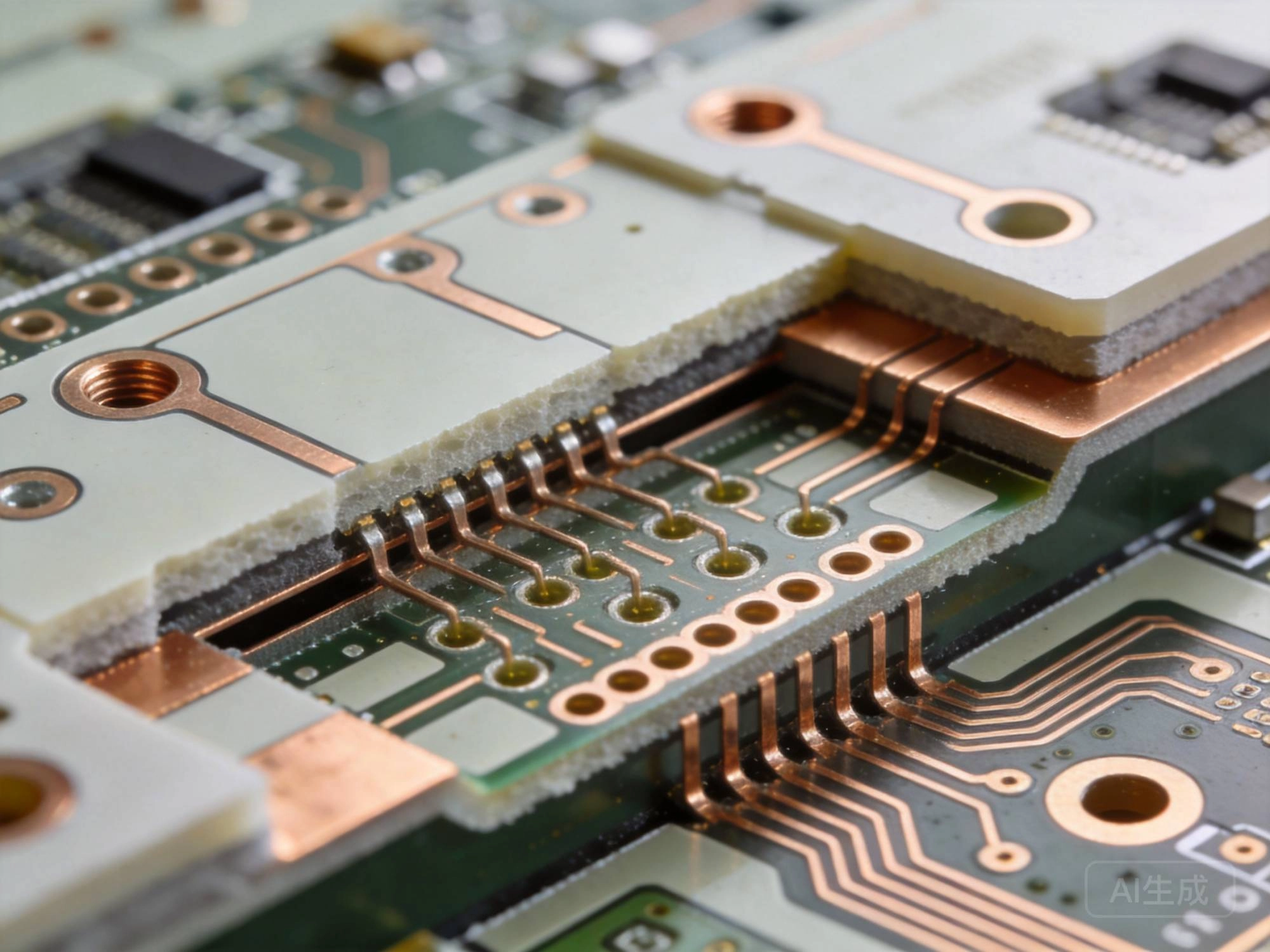
To understand the value of these via types, it helps to first be clear about what makes them different from the standard through-hole via most people start with.
A standard through-hole via drills completely through all layers of a multilayer board, connecting the top surface to the bottom surface. It is the workhorse of PCB interconnect — simple to fabricate and universally supported. But it consumes routing space on every layer it passes through, which becomes a real problem when you need to fit more into less area.
A Blind Via connects an outer layer to one or more inner layers without drilling through the entire board. It starts at an outer surface and stops at a specified internal layer. From the outside, you can see the via opening, but you cannot see where it terminates — hence the name "blind."
Blind vias allow designers to route signals from an outer layer directly into the board's interior without sacrificing routing channels on the layers in between. This is especially valuable near high-pin-count components like BGAs, where routing channels are at a premium.
A Buried Via is hidden completely — it connects internal layers only, with no connection to either outer surface. You cannot see it from the top or bottom of the board. Buried vias are used to create dense interconnection networks within the inner layer stack, freeing up space on the outer layers for component placement and signal routing.
The combination of blind and buried vias is what enables HDI (High-density Interconnect) board designs to achieve routing densities that would be impossible with through-hole vias alone. The term "Any-layer Hdi" refers to designs where micro blind vias are used on every interlayer connection, giving designers maximum flexibility in routing.
Fabricating blind and buried vias requires additional process steps beyond standard multilayer board production, and the method chosen has a direct impact on cost, minimum feature size, and board reliability.
The most common method for creating blind and buried vias is Sequential Lamination. The board is built up in stages:
Each additional lamination cycle adds cost and some risk of delamination, so designs with many sequential buildup steps require careful process control and high-Tg base materials.
Modern HDI boards use laser ablation to form microblind vias, typically 60–150 micrometers in diameter. Laser drilling offers several advantages over mechanical drilling for via formation:
CO2 lasers are typically used for dielectric ablation, while UV lasers provide higher precision for very small microvias in advanced applications. The choice of laser type depends on the via depth, the dielectric material, and the required aspect ratio.
Once the via hole is formed, it must be metallized. For microblind vias, this typically involves electroless copper plating followed by electroplated copper to build up the barrel wall. The plating process must achieve void-free coverage to ensure reliable connectivity, especially in thermal cycling conditions.
After plating, microblind vias are often filled with a non-conductive fill material and plated over to create a flat surface suitable for component mounting. This is particularly important for via-in-pad applications, where the via sits directly under a BGA pad or a passive component termination.
Getting the most out of blind and buried vias requires paying attention to a set of design rules that differ from standard multilayer board guidelines.
Laser-drilled microblind vias can be as small as 60 µm in diameter, though 100 µm is more common in production. The associated capture pad on the target layer typically needs to be at least 3 times the via diameter. Via-to-via spacing should be at least one via diameter to avoid drill breakout or plating uniformity issues.
The aspect ratio — the ratio of board thickness to via diameter — is a key constraint for blind via formation. Laser drilling can typically achieve depth-to-diameter ratios of up to about 1:1 reliably, though controlled-depth laser processes can push this to roughly 1.5:1. Through-hole vias, by contrast, routinely achieve aspect ratios of 10:1 or higher with mechanical drilling.
One of the trickiest aspects of designing with blind and buried vias is keeping track of which layers connect to which. In a complex HDI stack, a single net might pass through several different via types to travel from component pad to destination. Designers need to carefully document the layer connectivity matrix and verify it against the fabrication vendor's capabilities.
Software tools with HDI-aware stackup planning can help manage this complexity, but it is still one of the areas where close collaboration between the designer and the manufacturer pays off most.
Because blind and buried vias are often placed under BGAs and near other heat-generating components, they experience significant thermal stress during operation and assembly reflow. The thermal coefficient of expansion (TCE) mismatch between the copper via barrel and the surrounding dielectric can cause fatigue cracks over thermal cycling.
Design mitigations include using high-Tg or polyimide base materials, controlling plating thickness uniformity, and avoiding sharp corners in the via barrel through careful desmearing and etch-back processes. Manufacturers with well-tuned Sequential Lamination processes and robust plating Quality Control will deliver more reliable results over the product lifetime.
HDI boards are classified into types based on the number of buildup layers and the via technology used. This classification helps designers and manufacturers align on expectations:
As the type number increases, so does the cost per square centimeter and the process complexity. Choosing the right type is a balancing act between density requirements, budget, and production volume.
Blind and buried via technology shows up in products where space is at a premium and reliability cannot be compromised.
The most visible application of HDI and microblind via technology is the modern smartphone. Every millimeter of board area saved through blind and buried via routing allows for a larger battery, additional sensors, or a thinner enclosure. The same technology carries over to smartwatches and wireless earbuds, where extreme Miniaturization is the primary design driver.
Implantable medical devices such as pacemakers, neurostimulators, and hearing aids operate in physically constrained environments inside the human body. These devices use HDI boards with microblind vias not just for size reduction but also to enable high-channel-count sensing and stimulation arrays within a volume that must fit comfortably in the target anatomical location.
Advanced driver assistance systems (ADAS) modules, instrument clusters, and in-vehicle infotainment units all require increasingly dense boards to support the growing number of sensors, processors, and wireless interfaces in modern vehicles. HDI boards with blind and buried vias help Automotive Electronics suppliers meet the space and weight constraints imposed by vehicle design teams while maintaining the high reliability standards required by Aec-q100 and similar automotive qualification standards.
While not always thought of as HDI applications, high-speed server boards and network switch cards use blind and buried via structures to manage dense differential pair routing and to minimize via stub effects that degrade signal quality at data rates above 25 Gbps. Buried via technology lets signal layers sit close to the reference planes without sacrificing routing channels on the outer layers.
There is no getting around the fact that blind and buried vias add cost to a PCB. The additional sequential lamination cycles, laser drilling steps, and plating processes all contribute to a higher per-board price compared to a standard through-hole multilayer board of the same overall dimensions.
That said, the cost equation changes when you account for what you are getting in return. Using blind and buried vias can allow a smaller board to do the job of a larger one, reducing enclosure size, material costs, and assembly complexity. In high-volume consumer products, those savings often far outweigh the incremental PCB Fabrication cost.
For low-to-medium volume industrial and medical applications, the decision tends to come down to whether the density requirement is real and whether the additional manufacturing cost fits within the product's bill of materials. Prototyping runs with sequential lamination and microblind vias are more expensive per board, but they are often the only viable path to a working design in highly constrained packages.
If your design requires blind and buried vias, the single most important thing you can do is engage your PCB manufacturer early in the design cycle. Not all fab houses have the same capabilities, and the gap between what is achievable in a state-of-the-art HDI facility versus a standard multilayer shop is enormous.
Before sending files, confirm the following with your vendor:
A manufacturer with a mature HDI process will typically provide a Design For Manufacturing (Dfm) review that flags any rules violations before production starts. This step alone can save weeks of rework and respin delays.
Blind and buried vias are foundational technologies for anyone working with high-density electronics. They enable board-level Miniaturization that is simply not possible with through-hole vias alone, and they unlock routing strategies that keep signal paths short and clean in compact, high-performance designs.
The trade-off is added process complexity and cost, but for products where space, weight, and performance matter — consumer wearables, medical implants, automotive modules, and high-speed compute — that trade-off is usually worth making. The key is to understand the fabrication requirements, follow the design rules carefully, and work closely with a manufacturer who has proven HDI capabilities.
Contact us to discuss your requirements.

Wearable Health Monitors: The Importance of Biocompatible Flex PCBsSeptember/02/2026

Sustainability in PCB Fabrication: Eco-Friendly Materials and ProcessesJuly/01/2026
How DFM Analysis Saves You Money on Multilayer PCBsAugust/19/2026
The Hidden Costs of Cheap PCBs: Why Quality MattersJuly/23/2026
What is Rigid-Flex PCB? Complete Guide from China ManufacturerMay/18/2026

Detailed Explanation of the Types, Materials, and Applications of Flexible Circuit Boards 101June/04/2026
How to Prevent Common Failures in Flexible Circuit DesignSeptember/09/2026
Metal Core PCB (MCPCB) Basics: Aluminum vs. Copper SubstratesSeptember/29/2026