Open Nav

If you've ever wondered how those impossibly dense printed circuit boards inside your smartphone or tablet come to life, you're not alone. The Hdi Pcb Manufacturing process is one of the most sophisticated operations in modern electronics production—a carefully orchestrated sequence of precision steps where fractions of millimeters matter and every decision impacts final performance.
As an experienced Hdi Pcb manufacturer, we've refined these processes over thousands of production runs. In this comprehensive guide, we'll walk you through each stage of Hdi Pcb Manufacturing, explaining not just what happens but why each step matters for your final product.
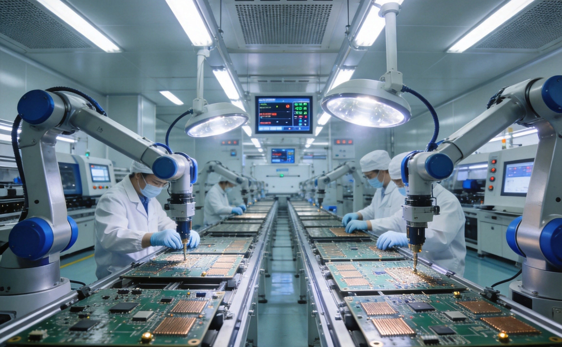
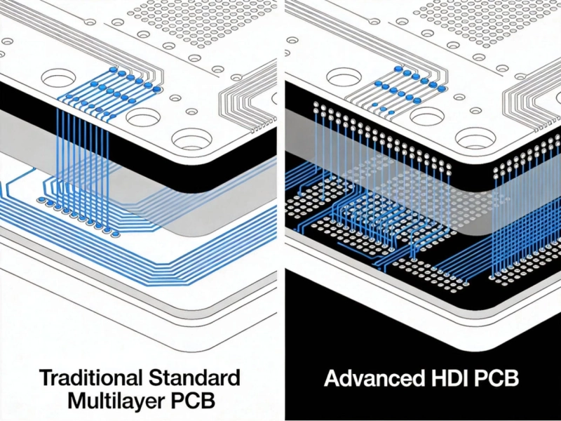
Before diving into specifics, let's establish why Hdi Pcb manufacturing differs fundamentally from standard Pcb Production. Traditional PCBs rely on mechanical drilling and through-hole vias that connect every layer. HDI Pcb Manufacturing introduces sequential build-up layers with laser-drilled Microvias, enabling routing densities that simply aren't possible with conventional methods.
The complexity increases exponentially. Where a standard 6-layer PCB might involve 10-15 distinct process steps, a complex Any Layer HDI board can require 40-50 steps, each demanding precise control. Understanding this process helps you appreciate the value good manufacturers bring—and what questions to ask when evaluating partners.
Our manufacturing facilities have processed millions of HDI boards across various complexity levels. We've learned that quality isn't accidental—it's engineered into every step from initial design review through final inspection.
HDI Pcb Manufacturing begins long before actual board processing. Material selection significantly impacts final electrical performance, thermal characteristics, and manufacturing yields. For most HDI applications, we work with:
Material lot traceability is critical. We maintain complete records linking each production panel to its source material, enabling rapid diagnosis if any issues emerge during testing or field operation.
Raw laminate sheets arrive in standard panel sizes (typically 18" x 24" or 21" x 25"). The first manufacturing step cuts these sheets to your specific board dimensions, accounting for production panel efficiency while meeting your size requirements.
Cut panels undergo visual inspection and dimensional verification. Any panels with defects—scratches, delamination, contamination—are rejected before processing begins. This upfront Quality Control prevents wasted processing on compromised material.
For multilayer HDI boards, inner layer circuitry must be formed before build-up layers are added. This involves:
Inner layer registration is particularly critical for HDI. Misalignment here compounds through subsequent build-up layers, potentially causing opens or shorts in the finished board. Our facilities use precision optical registration systems achieving alignment accuracy within 15μm.
After inner layer formation, copper surfaces are treated with anti-oxidation coating to prevent degradation during storage and subsequent processing. Layers are then stacked with precise alignment, separated by prepreg (pre-impregnated fiberglass) layers that will flow and cure during lamination.
Layer count, thickness, and prepreg selection are determined by your Stackup Design—a critical engineering decision affecting impedance, thermal performance, and manufacturing robustness. This is where manufacturer expertise directly impacts your board's electrical behavior.
Layer stack-up enters our hydraulic lamination presses, where controlled temperature and pressure cycles cure the board. Standard parameters include:
Modern HDI manufacturing uses computer-controlled presses with closed-loop feedback, ensuring consistency across panel batches. We've seen boards from older equipment fail where modern controlled systems produce repeatable excellence.
HDI PCB manufacturing uses two complementary drilling technologies:
Mechanical drilling handles through-holes and larger vias (typically above 0.15mm). Computer-controlled drill machines with precision-spindles and carbide bits achieve high speed and accuracy. Critical parameters include:
Laser Drilling creates the Microvias that define Hdi Technology. UV and CO2 laser systems ablate dielectric material with precision measured in microns. This is where HDI manufacturing diverges fundamentally from standard Pcb Production.
After drilling, every hole requires copper plating to create electrical connections. Before plating, the hole walls must be perfectly clean—a process called desmear removes any resin smear or heat-affected zones from drilling.
Desmear involves sequential chemical treatment:
Following desmear, electroless copper deposition creates a thin conductive seed layer (typically 0.3-0.5μm) on all exposed surfaces including hole walls. This seed layer enables subsequent electrolytic copper plating to build up the required thickness.
Panel plating deposits copper uniformly across the entire board surface and inside all holes. Modern plating lines use reverse-pulse plating to achieve superior throwing power—the ability to deposit metal uniformly even in high aspect-ratio features.
Plating thickness targets are established by design requirements. Standard HDI boards typically require 18-25μm copper on surface traces and minimum 20μm in through-hole barrels. We verify thickness at multiple points across each panel using X-ray fluorescence (XRF) instruments.
This is the heart of HDI PCB manufacturing—the sequential build-up that distinguishes High Density Interconnect from conventional multilayer boards. Each build-up cycle adds a layer of routing density through a carefully controlled sequence.
Each build-up layer involves multiple sub-steps:
The number of build-up cycles depends on your HDI structure—1-N-1 uses one cycle per side, while Any Layer HDI may involve 4-6+ cycles per side. Each cycle adds time, cost, and opportunity for variation.
Build-up layers start by laminating thin dielectric material over the existing circuitry. Options include:
Lamination uses lower pressure than core pressing, just enough to ensure void-free contact without disturbing underlying circuitry. Temperature is carefully controlled to prevent premature curing or foil wrinkling.
After dielectric lamination, laser systems create microvias that connect the new surface layer to underlying circuitry. This is where HDI manufacturing requires substantial capital investment and technical expertise.
Laser types used in HDI manufacturing:
Key microvia parameters:
Laser Drilling rates are impressive—modern systems drill thousands of vias per minute. But setup and optimization require significant expertise. Via shape, debris removal, and consistent depth all affect final quality. We've invested heavily in laser capability and operator training—this step often determines the difference between adequate and excellent HDI production.
After laser via formation, desmear and electroless copper deposition create the seed layer for via plating. Flash plating then deposits copper inside the newly formed microvias.
Microvia plating is particularly challenging because:
Many manufacturers use fill plating processes that deposit copper preferentially inside vias, achieving void-free fill without excessive surface buildup. This "via-in-pad" capability is essential for modern high-density designs.
With vias filled and flashed, pattern formation follows the same process as inner layers: photoresist application, exposure, development, etching, and stripping. Build-up layer patterns use finer design rules—typically 50-75μm traces compared to 100μm+ on standard layers.
Aoi inspection at this stage catches any defects before they compound through subsequent build-up cycles. Finding an issue after 4 build-up layers is far more costly than catching it after the first.
After completing required build-up layers, outer layer patterns are formed using the same photolithography process. For outer layers, we must also handle:
Solder mask serves multiple purposes: protecting copper traces from oxidation, preventing solder bridges during assembly, and providing the characteristic green (or other color) appearance. For HDI boards, liquid photoimageable (LPI) solder mask is standard due to its fine resolution capability.
Solder mask process steps:
For fine-pitch components common on HDI boards, solder mask dams must be precisely controlled. We regularly achieve mask dams below 50μm—critical for preventing bridges on high-density BGA packages.
The surface finish protects exposed copper pads while providing a solderable surface for component assembly. Common options for HDI include:
For most high-density HDI applications, we recommend Enig for its superior flatness and compatibility with fine-pitch assembly. Gold thickness (typically 1-3μm over 150-200μm nickel) is carefully controlled to prevent durability issues.
Component designators, revision codes, company logos, and other markings are applied via legend printing. Modern systems use inkjet or laser marking for precision and durability. These markings must remain legible through assembly and product life while not interfering with component placement.
Individual boards are cut from production panels using CNC routers or laser cutting systems. CNC routing offers good precision and edge quality for most applications:
For complex shapes or tight tolerances, laser cutting offers superior precision. Some manufacturers use combined approaches—CNC for rough profiling, laser for final dimensions.
For high-volume production where cost is paramount, V-scoring offers faster depanelization than routing. A V-shaped blade cuts partial-depth grooves on panel top and bottom, leaving connecting tabs that break cleanly after assembly.
V-scoring requires careful design considerations:
Whether by router or V-score break, depanelization separates finished boards from production panels. Automated depanelization systems minimize stress on boards, while manual breaking is reserved for low-quantity or complex shapes.
Every HDI PCB we produce undergoes comprehensive electrical testing. Flying probe testers use spring-loaded probes that make temporary contact with test points, verifying:
Flying probe offers advantages for complex HDI designs where bed-of-nails fixtures are impractical. Test coverage approaches 100% of accessible nodes.
AOI systems use high-resolution cameras and sophisticated software to inspect boards for defects:
AOI catches visual defects that electrical testing cannot see. For HDI boards with fine features, AOI resolution must be correspondingly high—we use systems with 5-10μm resolution capable of detecting defects invisible to earlier generation equipment.
For critical applications or when questions arise, we employ destructive analysis methods:
These tests are typically performed on sample basis rather than 100% of production, but demonstrate our commitment to understanding and proving process capability.
Before shipping, trained inspectors perform final visual examination of every board, looking for issues that automated systems might miss:
This human oversight adds a layer of Quality Assurance that automated systems cannot replicate, particularly for boards destined for visible applications or premium products.
HDI boards are packaged in clean, controlled environments to prevent contamination and damage. Standard packaging includes:
For moisture-sensitive devices (MSD), we follow J-STD-033 guidelines, including dry storage and specified exposure limits before assembly baking.
Each shipment includes comprehensive documentation:
We maintain records for minimum 3 years, enabling traceability long after boards ship. This documentation proves invaluable when questions arise months or years later.
As build-up layers accumulate, registration tolerance stacks compound. A 15μm misalignment on layer 1 becomes a 30μm issue on layer 3, and potentially a 45μm problem on layer 5. Managing this accumulation requires:
Microvias in build-up layers face thermal stress concentrations during assembly and operation. Reliability depends on:
We've developed proven via designs and process parameters through extensive testing. For automotive and medical applications, we perform additional thermal cycling and pull testing to verify reliability.
Build-up dielectric thickness affects impedance, clearance, and overall board thickness. Variation sources include:
Modern materials and processes achieve ±10% thickness control, but designers must account for this variation in critical impedance calculations.
Mature HDI manufacturers track statistical process capability:
Ask potential manufacturers about their actual yields and defect rates:
Reputable manufacturers share these metrics openly. If a supplier hesitates to provide data, that should raise concerns.
Typical lead times from order confirmation to shipment:
These timelines assume no complications. Complex designs with unique requirements may need additional engineering time.
Minimum order quantities depend on board complexity and manufacturer. Typical ranges:
Many manufacturers offer prototype quantities at higher per-unit cost. For production, minimums are more reasonable due to setup cost amortization across larger batches.
Relevant standards include:
For most commercial applications, compliance with IPC-6012 Class 2 or 3 is sufficient. Automotive, medical, and aerospace applications require additional testing and documentation.
Key recommendations:
We've seen countless designs that required respins due to avoidable issues. Early manufacturer engagement almost always pays for itself.
Any Layer HDI (ALH) represents the highest complexity HDI structure where any layer can connect to any other layer through blind and Buried Vias. Manufacturing differences:
The decision between standard HDI and ALH should weigh density requirements against cost and yield implications.
HDI PCB manufacturing represents the intersection of precision engineering, advanced materials science, and sophisticated process control. Every board that ships from our facility has passed through dozens of critical steps, each demanding expertise and attention to detail.
Understanding this process helps you make better decisions as an engineer or product manager. You can ask informed questions, understand trade-offs, and appreciate why quality HDI manufacturing commands premium pricing. More importantly, you can select manufacturing partners who invest appropriately in the capabilities that matter for your specific application.
Whether you're designing the next generation smartphone, an automotive safety system, or a medical diagnostic device, the principles of HDI manufacturing remain constant. Choose partners who understand these principles—who can explain their processes, demonstrate their capabilities, and prove their quality through data rather than promises.
Ready to discuss your HDI PCB manufacturing requirements? Upload your design files for a free Dfm review and quotation. Our engineering team will provide detailed feedback on manufacturability, cost optimization, and timeline—helping you bring your high-density design to life with confidence.
Top 5 Applications of HDI PCBs in Modern ElectronicsMay/13/2026
How to Choose the Best China HDI PCB Manufacturer in 2026June/08/2026
What is the Minimum Trace Width for HDI PCBs?July/17/2026
The Ultimate Guide to HDI PCB Technology You Need to KnowJune/02/2026
Understanding HDI PCB Technology: A Comprehensive Guide for BeginnersMay/13/2026
HDI PCB vs Standard PCB: Key Differences ExplainedMay/13/2026
What is HDI PCB? A Complete Guide from China HDI PCB ManufacturerMay/13/2026
Why Choose a China HDI PCB Manufacturer for Your Project?May/13/2026