Open Nav

If you've heard the term "Hdi Pcb" mentioned in electronics discussions but found the explanations overly technical, you're in exactly the right place. This guide breaks down HDI Pcb Technology into plain language anyone can understand—no engineering degree required.
As your friendly introduction to High Density Interconnect technology, we'll start from the absolute basics and build up your understanding step by step. By the end, you'll grasp why HDI PCBs matter, where they're used, and why they're transforming modern electronics.
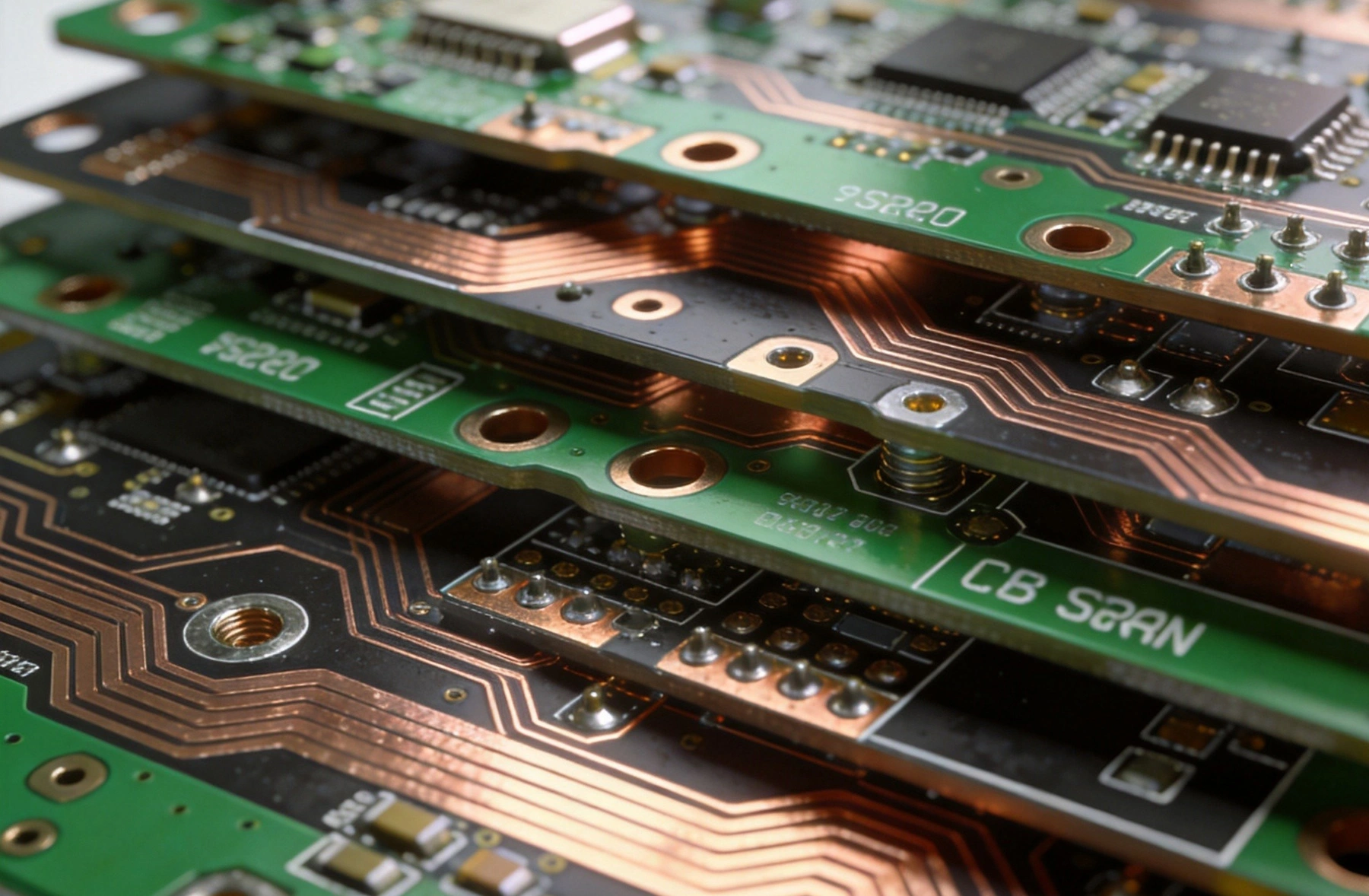
HDI stands for High Density Interconnect. It's a way of building printed circuit boards (PCBs) that packs more circuitry into a smaller space compared to traditional methods.
Think of it like comparing a single-lane country road to a multi-lane highway. Both move cars from point A to point B, but the highway handles far more traffic in the same distance. HDI PCBs work the same way—they move electrical signals more efficiently while taking up less space.
The technology became essential as devices shrank while becoming more powerful. Your smartphone contains more computing power than the room-sized computers of the 1970s—and much of that achievement comes from HDI Pcb Technology.
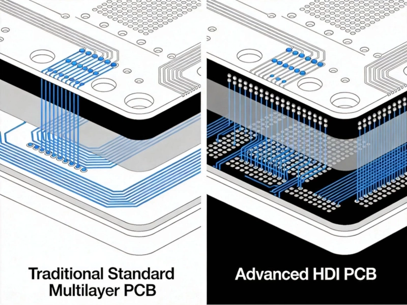
To understand why HDI matters, let's first look at how traditional PCBs work. A standard Multilayer Pcb connects layers using through-hole vias—imagine drilling a hole all the way through a stack of papers and then threading a wire through every single page.
This approach works fine when you have plenty of space. But what happens when you need to fit the circuitry of a smartphone inside a case thinner than a centimeter?
Traditional PCBs face several limitations:
These limitations aren't problems for many applications. Industrial equipment, automotive controls, and many other products work perfectly fine with traditional PCBs. But for compact consumer electronics, medical devices, and advanced communications equipment, HDI often becomes essential.
At the heart of Hdi Technology lies the microvia. Unlike traditional through-hole vias that drill completely through a board, Microvias only go partway through—connecting specific layers rather than all layers.
Picture our paper stack example again. Instead of threading a wire through every page, you'd create small connections only between the pages that actually need to communicate. This saves space and reduces unnecessary connections.
Microvias are typically:
These tiny connections enable routing densities impossible with conventional technology. The difference is similar to fitting more highways under a city's street level—suddenly you can move far more traffic without expanding the surface area.
HDI PCBs use several via types working together:
Through-hole vias remain part of HDI designs but serve different purposes than in traditional boards. They handle connections that truly span the entire board while microvias handle local high-density routing.
Blind Vias connect an outer surface layer to inner layers without breaking through to the other side. If you need to connect layer 1 to layer 3, a Blind Via stops exactly at layer 3—nothing extends further.
Buried Vias connect only inner layers and remain completely hidden from both board surfaces. These invisible connections enable incredible density by allowing routing anywhere on inner layers.
Stacked vias directly stack microvias on top of each other, creating vertical connections through multiple layers. This advanced technique further increases density but requires precise manufacturing control.
Skip vias jump over one or more layers to make distant connections. A skip via from layer 1 to layer 5 bypasses layers 2, 3, and 4—useful for power and ground connections in complex designs.
Understanding HDI structures starts with the concept of "build-up layers." Imagine a traditional PCB core as the foundation of a building. Hdi Technology then adds additional floors (build-up layers) on top of this foundation.
Each build-up layer adds routing space without increasing board footprint. This is precisely why HDI enables Miniaturization—more usable area without changing the board's size.
1-N-1 (One Build-Up)
The simplest HDI structure adds one routing layer on each side of the core. Think of it as adding a single floor above and below the ground floor. This structure provides meaningful density improvement while remaining relatively straightforward to manufacture.
Typical applications include mid-range smartphones, basic IoT devices, and Automotive Electronics where moderate density improvements suffice.
2-N-2 (Two Build-Up Layers)
This structure adds two routing layers on each side of the core—effectively doubling the available routing area. Manufacturing complexity increases but so does design flexibility.
Most flagship smartphones from a few years ago used 2-N-2 HDI. The technology provides an excellent balance between density and manufacturing cost.
Any Layer HDI (ALH)
The most advanced structure treats all layers equally, with any layer able to connect to any other layer through blind and Buried Vias. This maximum flexibility enables the highest possible routing density.
Current flagship smartphones, the latest tablets, and advanced medical devices use Any Layer HDI. Apple famously uses this technology in iPhone mainboards—it's what enables the dense circuitry powering Face ID and computational photography.
You might encounter HDI structures written as "1-N-1," "2-N-2," or similar notations. Here's how to interpret them:
A 4-layer 1-N-1 board has: 1 build-up layer + 2 core layers + 1 build-up layer = 4 total layers
An 8-layer 2-N-2 board has: 2 build-up layers + 4 core layers + 2 build-up layers = 8 total layers
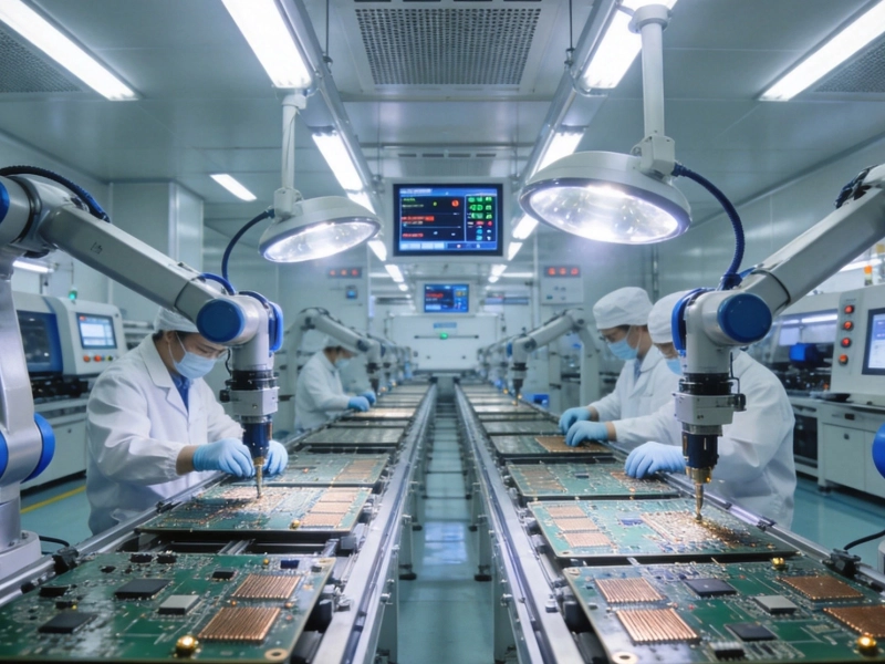
Understanding manufacturing helps you appreciate why HDI costs more than traditional PCBs. The basic process includes:
Core preparation follows traditional Multilayer Pcb methods. Inner layers are patterned, inspected, and stacked with prepreg before press lamination.
Mechanical drilling creates through-holes for connections spanning all layers. These holes are then plated with copper using chemical deposition and electroplating.
Build-up layer lamination adds thin dielectric material over the existing circuitry. This step separates new routing layers from underlying connections.
Laser Drilling creates the microvias defining HDI technology. Specialized UV or CO2 laser systems ablate dielectric material with incredible precision, creating holes measured in hundredths of millimeters.
Via filling and plating deposits copper inside microvias, creating electrical connections between layers. This step requires sophisticated plating chemistry and process control.
Pattern formation creates the actual circuit traces on each build-up layer, following the same photolithography process used in traditional Pcb Manufacturing.
Surface finishing and testing applies protective coatings, performs electrical verification, and inspects final boards for defects.
The key difference from traditional manufacturing: HDI requires repeating the build-up, laser drill, and plating steps for each additional layer. A complex Any Layer HDI board might undergo this cycle six or more times—explaining the higher cost compared to simpler designs.
Traditional PCB drilling uses mechanical bits—essentially miniature versions of the drill bits in your workshop. These bits wear quickly when drilling small holes and struggle below certain sizes.
Laser Drilling uses focused light energy to remove material. This approach enables:
The capital equipment for laser drilling represents a significant investment—millions of dollars per system. This investment contributes to higher HDI manufacturing costs but enables capabilities impossible with mechanical drilling alone.
The most obvious benefit: HDI enables smaller, lighter products. A smartphone mainboard using Any Layer HDI can be 30-40% smaller than an equivalent traditional Pcb Design.
This size reduction directly translates to thinner, lighter devices. Every millimeter shaved from Circuit Board thickness potentially allows a thinner product case or larger battery—both significant competitive advantages.
Beyond size, HDI provides electrical advantages:
Better Signal Integrity comes from shorter via lengths. Microvias create smaller stubs that cause less Signal Reflection and loss at high frequencies. This matters enormously for 5G communications, high-speed computing, and RF applications.
Reduced inductance and capacitance from smaller vias improves power distribution and reduces noise. High-speed digital designs benefit significantly from these improvements.
Design flexibility increases because engineers can route signals more efficiently. Critical nets can take optimal paths rather than being constrained by through-hole limitations.
Counterintuitively, HDI can improve thermal performance in some ways:
Thermal engineers often find creative HDI solutions outperform traditional approaches in compact thermal packages.
HDI enables higher component density through:
Modern smartphones pack thousands of components onto boards smaller than your palm—impossible without HDI technology.
Smartphones represent the largest HDI application by volume. Every flagship phone uses Any Layer HDI for main processors, RF modules, and camera systems. Tablets, smartwatches, wireless earbuds, and fitness trackers similarly depend on HDI.
The relentless consumer demand for thinner, lighter, more capable devices drives HDI adoption. Without HDI, current smartphone designs simply wouldn't fit inside their cases.
Modern vehicles contain dozens of electronic control units (ECUs), infotainment systems, and advanced driver assistance systems (ADAS). These systems require:
Automotive HDI applications range from dashboard displays to engine control modules. Quality requirements exceed consumer electronics—automotive boards must function reliably for 10+ years under harsh conditions.
Medical electronics demand Miniaturization for patient comfort and device portability:
Medical device manufacturers choose HDI for the same reasons as consumer electronics—smaller size and lower weight matter enormously for wearable and implantable products.
5G infrastructure and high-speed networking equipment use HDI for:
These applications require both the density HDI provides and the Signal Integrity improvements from reduced via stubs.
IoT devices span the full range from simple sensors to complex edge computing systems. HDI usage varies by complexity:
The IoT explosion drives significant HDI demand as manufacturers compete to make devices smaller, more capable, and more affordable.
HDI technology makes sense when:
Traditional PCBs remain the better choice when:
Modern designs often combine both technologies:
This hybrid approach optimizes both cost and performance by using each technology where it makes most sense.
Stackup: The vertical arrangement of layers in a PCB, including thickness, material, and copper weight of each layer. HDI stackups are more complex than traditional designs.
Build-up sequence: The order in which HDI layers are added during manufacturing. This sequence affects registration tolerances and overall quality.
Via aspect ratio: The ratio of via depth to diameter. Higher aspect ratios are more difficult to plate reliably.
Land pad: The copper pad surrounding a via connection point. Landing size affects reliability and manufacturability.
Capture/latch ratio: The ratio of pad size to via diameter. Larger ratios improve manufacturing yield and reliability.
International standards define HDI quality requirements:
Working with manufacturers familiar with these standards ensures your designs meet industry quality expectations.
HDI design rules differ from traditional Pcb Design:
Always obtain design rules from your specific manufacturer—they have different capabilities within the HDI spectrum.
Design For Manufacturability (Dfm) review is essential for HDI. This engineering review:
Reputable HDI manufacturers offer Dfm review as a standard service. This investment typically prevents costly respins due to manufacturing issues.
HDI materials include options beyond standard FR-4:
Material choice affects cost, manufacturability, and electrical performance. Discuss options with your manufacturer early in design.
Several factors contribute to higher HDI pricing:
Despite higher costs, HDI often reduces overall system cost by enabling smaller enclosures, fewer boards, and simplified assemblies.
Strategies to optimize HDI cost-effectiveness:
Quality verification for HDI includes:
Electrical testing verifies all connections are correct using flying probe testers. These systems test nets without requiring custom fixtures—essential for complex HDI designs.
Aoi (Automated Optical Inspection) catches visual defects like pattern issues, solder mask problems, and surface defects. High-resolution Aoi is critical for detecting fine-feature problems.
X-ray Inspection reveals internal structure including via fill quality and hidden defects. This non-destructive method catches issues invisible to external inspection.
Cross-section analysis destructively examines internal structure. Samples are potted, polished, and examined under magnification to verify plating quality, registration, and layer structure.
Thermal cycling tests board reliability under temperature stress. This accelerated life testing verifies HDI boards will survive expected field conditions.
Before selecting an HDI supplier, ask about:
Current HDI technology typically achieves microvias as small as 0.1mm (100μm). Advanced manufacturing can produce 0.075mm vias, though production yields decrease at this extreme. For practical production, 0.1mm represents the sweet spot for most applications balancing density with yield.
HDI can reduce board area by 20-50% depending on the complexity comparison. Any Layer HDI designs typically achieve 30-40% size reduction versus equivalent traditional multilayer designs. The actual savings depend on your specific design density and the HDI structure chosen.
When properly designed and manufactured, HDI achieves equivalent or superior reliability to traditional PCBs. Microvias actually eliminate some failure modes present in through-hole designs. For automotive and medical applications requiring high reliability, HDI with proper qualification testing performs excellently.
HDI handles power distribution adequately for most digital and mixed-signal designs. For very high current applications requiring thick copper (>3oz), traditional PCB construction may offer advantages. However, hybrid approaches can combine HDI density for signal routing with traditional power planes for high-current paths.
HDI refers broadly to any high density interconnect technology using microvias. Any Layer HDI (ALH) represents the highest complexity HDI structure where any layer can connect to any other layer. ALH requires more manufacturing steps, tighter tolerances, and costs more than simpler HDI structures—but provides maximum design flexibility.
You've now completed your introduction to Hdi Pcb technology. We covered the fundamentals: what HDI means, why microvias matter, how structures differ, where HDI is used, and how to decide if it's right for your project.
Key takeaways to remember:
Whether you're designing the next breakthrough consumer device, an automotive safety system, or a portable medical product, understanding HDI options helps you make informed decisions.
Ready to explore HDI for your next project? Our engineering team is available to discuss your requirements, answer questions, and provide guidance on whether HDI makes sense for your specific application. Upload your design files for a free Dfm Review—we'll help you understand your options without any obligation.
What is HDI PCB? A Complete Guide from China HDI PCB ManufacturerMay/13/2026
Top 5 Applications of HDI PCBs in Modern ElectronicsMay/13/2026
How to Choose the Best China HDI PCB Manufacturer in 2026June/08/2026
HDI PCB vs Standard PCB: Key Differences ExplainedMay/13/2026
What is the Minimum Trace Width for HDI PCBs?July/17/2026
Why Choose a China HDI PCB Manufacturer for Your Project?May/13/2026
The Ultimate Guide to HDI PCB Technology You Need to KnowJune/02/2026
HDI PCB Manufacturing Process: Step-by-Step ExplanationMay/13/2026