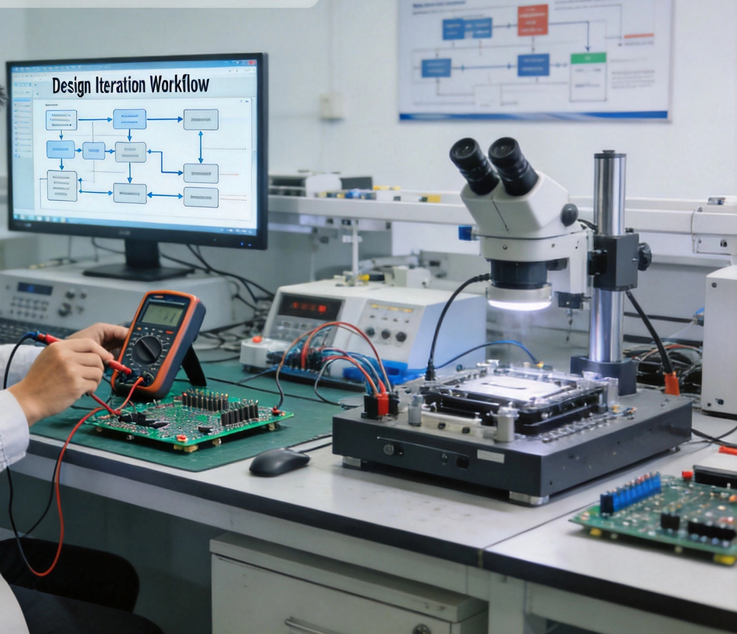
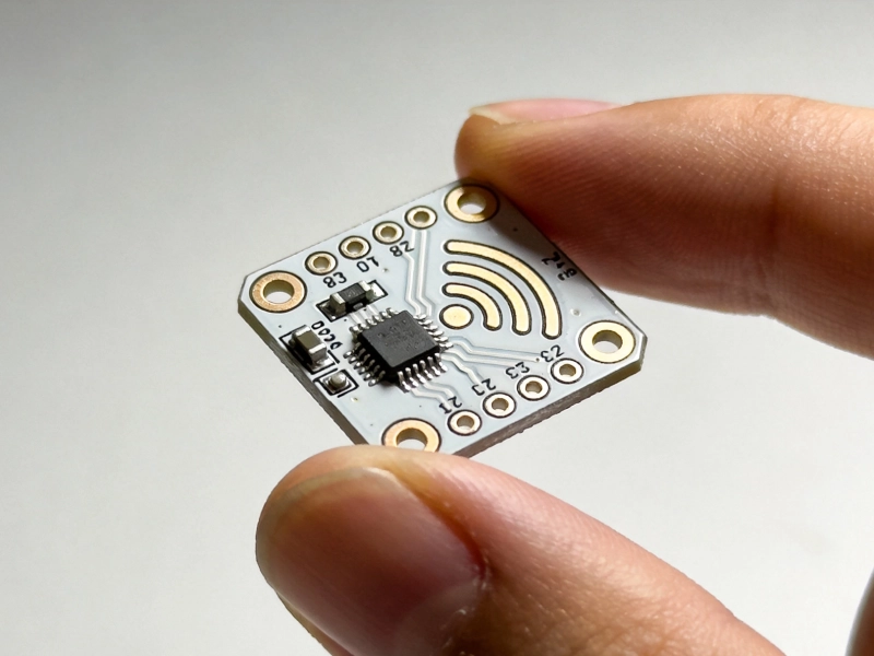
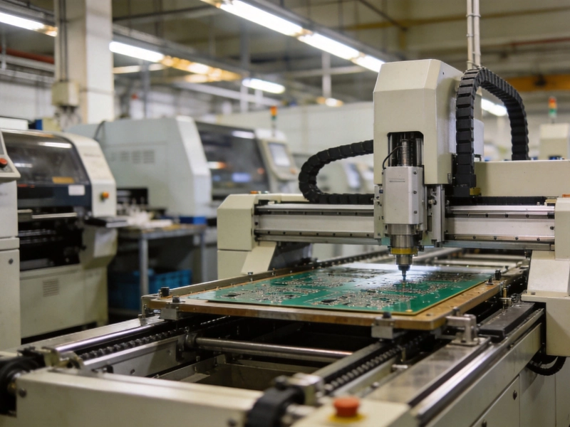
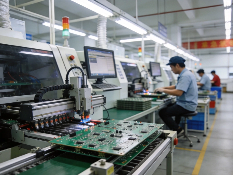
Your engineering team just finished the schematic design for a new IoT device. The pressure is mounting—your product launch deadline is approaching rapidly, and every day of design iteration means another delay. You need PCB prototypes fast, and you've heard about China's quick-turn capabilities but aren't sure how to navigate the process. This scenario plays out daily in electronics companies worldwide: design engineers need reliable prototype manufacturing with fast turnaround, Quality Assurance, and predictable costs. China's Pcb Prototype Manufacturing ecosystem has evolved specifically to address these needs, combining speed, quality, and cost-effectiveness in ways that few other regions can match.
From single-sided test boards to complex multilayer HDI prototypes, Chinese prototype manufacturers deliver boards in days rather than weeks. This guide walks you through the entire process—from selecting the right prototype supplier to managing design iterations, optimizing costs, and ensuring quality for your critical prototypes. Based on our experience supporting electronics companies from startups to Fortune 500 corporations, we're sharing practical insights that engineering teams can apply immediately.

Why Prototype in China?
The decision to prototype in China typically comes down to three factors: speed, cost, and capability. Let's break down each advantage:
- Rapid turnaround times: Standard prototype production in China completes in 3-5 days, with express options available in 1-2 days for urgent requirements. Compare this to typical 10-15 day lead times in North America or Europe, and the advantage becomes clear. For time-critical product development cycles, this speed difference directly impacts Time-to-market and competitive positioning.
- Cost-effective prototyping: Prototype Pcb Manufacturing costs in China typically range from 30-50% lower than equivalent quality from other regions. Lower labor costs, efficient supply chains, and high-volume equipment utilization enable competitive pricing even for small prototype quantities. This cost advantage allows more design iterations within budget constraints, improving final product quality through thorough testing and refinement.
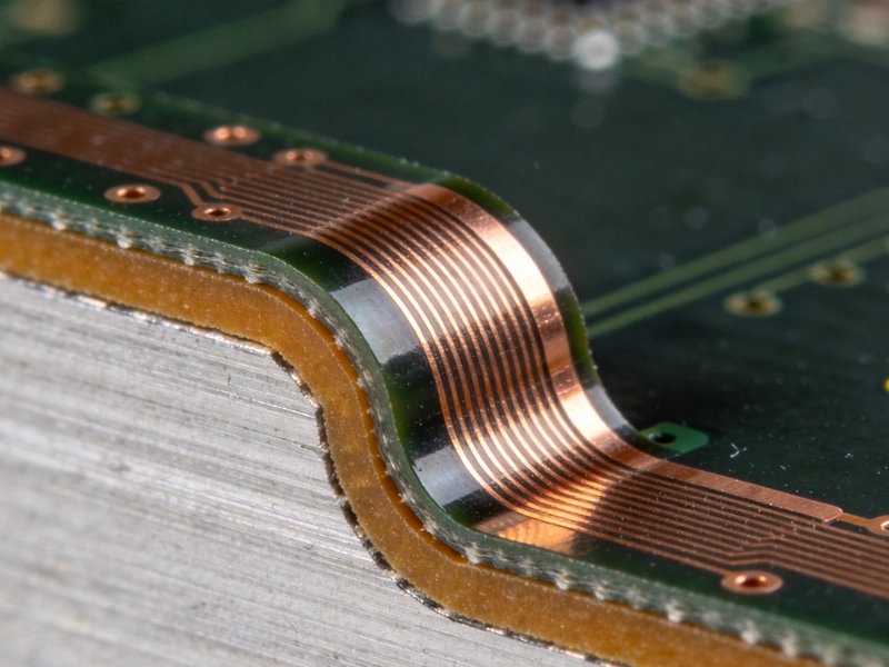
- Technology breadth: Chinese prototype manufacturers support virtually all PCB technologies—HDI boards with microvias, heavy copper up to 10+ oz, flexible circuits, rigid-flex assemblies, metal core boards, and specialized materials for high-frequency applications. For engineering teams exploring multiple technology options, finding suppliers with broad capability support simplifies the prototyping process.
- Quantity flexibility: Chinese prototype manufacturers specialize in small quantities from 1-10 pieces with no minimum order requirements. This flexibility enables multiple design iterations, functional testing of design variants, and parallel testing of alternative approaches—all without large upfront commitments or volume requirements.
- Design support services: Many Chinese prototype manufacturers provide engineering support including Dfm (Design For Manufacturing) reviews, Gerber file verification, Design Optimization suggestions, and troubleshooting assistance. This engineering support helps catch design issues early, reducing rework and accelerating the development process.
These advantages combine to make China the preferred choice for Electronics Prototyping worldwide. Companies from Silicon Valley startups to European automotive manufacturers rely on Chinese prototype capabilities to accelerate product development while maintaining quality standards and managing development costs effectively.
Prototype Manufacturing Process
File Preparation and Verification
Preparing design files correctly prevents delays and ensures first-time-right production. Essential files include:
- Gerber files: Standard RS-274X format for each copper layer, solder mask, silkscreen, and drill files—ensure layer mapping matches your design software output and naming conventions are clear
- Drill files: Separate drill file in Excellon format or included in Gerber files—specify drill sizes in metric or imperial units consistently and include drill legends if possible
- Fab drawings: Manufacturing drawings specifying board dimensions, tolerances, material requirements, copper weights, surface finish, and special instructions—critical dimensions should be clearly defined
- Assembly drawings: If assembly is required, BOM (bill of materials) and assembly drawings specifying component locations and reference designators
- Design specifications: Text specification document summarizing all requirements in one place for easy reference by manufacturing engineers
Many engineering teams make the mistake of sending incomplete file sets, resulting in clarification delays and potential errors. Taking time to verify file completeness and accuracy upfront saves significant time downstream. We provide free file verification services, identifying potential issues before production begins and requesting clarification where needed—typically within 2-4 hours of file receipt.
Production and Quality Assurance
Once files are verified, manufacturing follows standard Pcb Fabrication processes optimized for rapid prototype production:
- Material preparation: High-quality FR-4 materials (standard Tg 140°C or high-Tg 170°C+ for demanding applications) prepared for processing—material selection based on your specifications or recommendations if not specified
- Circuit imaging: Photoresist application, exposure through artwork, and development creating circuit patterns—prototype runs often use direct imaging eliminating phototools and accelerating the process
- Etching: Unprotected copper etched away leaving circuit patterns—careful process control ensures accurate trace widths and spacing
- Drilling: Mechanical drilling for standard holes and laser drilling for microvias in HDI boards—drilling parameters optimized for material type and hole size
- Plating: Electroless and electrolytic copper plating creating electrical connections between layers—critical for multi-layer boards
- Solder mask application: Protective coating applied to circuitry leaving exposed copper pads for component mounting—color options include green, black, blue, red, white, and transparent
- Surface finish application: Finish applied to exposed copper pads—Enig (electroless nickel immersion gold), Osp (organic solderability preservative), Hasl (hot air solder leveling), or other finishes per specification
- Electrical testing: 100% electrical testing verifying continuity and isolation—flying probe testing for prototypes, with bed-of-nails testing available for volume production
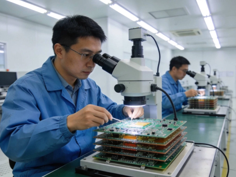
- Visual inspection: Visual inspection under magnification verifying solder mask registration, silkscreen alignment, and overall board quality
Prototype manufacturing emphasizes process control and verification at each step. Since prototypes often represent new designs with higher error risk, thorough testing prevents rework cycles that would delay development. We provide comprehensive test reports with each prototype shipment, including electrical test data and photographs of key board features.
Assembly Services
Many prototype projects require assembly services in addition to bare board fabrication:
- Component sourcing: Prototype manufacturers can source components from reputable distributors—specify authorized distributors for critical components or provide components yourself for proprietary parts
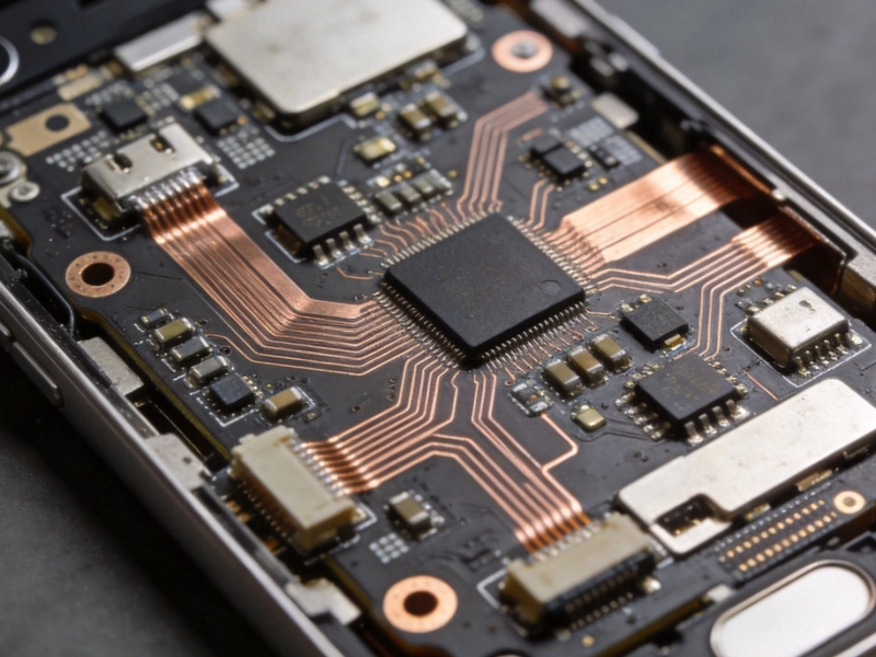
- Smt Assembly: Surface Mount Technology assembly using pick-and-place equipment and reflow ovens—supports fine-pitch components down to 0.3mm pitch with advanced equipment
- Through-hole assembly: Manual or automated through-hole component soldering for connectors, large components, or designs requiring through-hole components
- Mixed technology assembly: Combined SMT and through-hole assembly for designs using both component types on the same board
- Functional testing: Basic functional testing to verify assembled boards meet basic electrical requirements—comprehensive functional testing requires customer-provided test procedures
Prototype assembly enables faster design verification and reduces overall development time by eliminating separate bare board and assembly phases. We provide turnkey prototype assembly services with component sourcing, assembly, and basic functional testing—reducing coordination complexity for engineering teams.
Selecting Prototype Manufacturers
Capability Evaluation
Assessing prototype manufacturer capabilities requires understanding your specific requirements:
- Technology support: Verify the manufacturer supports your required technologies—HDI with microvias, heavy copper, flexible circuits, metal core boards, or specialized materials for high-frequency applications
- Layer count capability: Confirm maximum layer count supported—most prototype manufacturers handle up to 8-10 layers routinely, with some supporting 20+ layers for complex designs
- Feature size capability: Minimum Trace Width/spacing, via size, and other design features—ensure capabilities meet your design requirements, especially for advanced designs
- Surface finish options: Available finishes include Enig, Osp, Hasl, Immersion Silver, immersion tin—select appropriate finish based on assembly requirements and application environment
- Testing capabilities: Flying probe testing, electrical testing, Aoi (Automated Optical Inspection), x-ray inspection for microvias, impedance testing for controlled impedance designs
We recommend verifying capabilities through actual sample builds rather than relying solely on specification sheets. Request sample builds of representative designs to verify actual capability before committing to critical prototype projects. Our sample build service enables capability verification with minimal cost and risk.
Quality and Reliability
Prototype quality impacts downstream development significantly:
- Certification status: ISO 9001 certification indicates structured quality systems—essential for consistent prototype quality, especially for regulated industries
- First-pass yield: Ask about typical first-pass yield rates—higher yields indicate better process control and reduce rework delays
- Quality reporting: Detailed quality reports with test data and photographs provide visibility into prototype quality and enable confidence in test results
- Defect handling procedures: Clear procedures for handling defects and quality issues—critical for maintaining development schedules when problems occur
- Customer references: Request references from companies with similar applications and requirements—especially important for critical prototype projects
Low-quality prototypes waste time and budget—errors discovered during functional testing that trace back to fabrication defects cause unnecessary design iteration cycles. We maintain ISO 9001 certification and provide comprehensive quality reports with all prototype shipments, enabling traceability and confidence in manufacturing quality.
Communication and Support
Effective communication accelerates prototyping and reduces misunderstandings:
- Engineering support availability: Direct engineering support for design questions and manufacturing guidance—critical for complex designs or inexperienced teams
- Response time: Typical response time for file reviews, questions, and issue resolution—prototype projects require rapid communication
- Language capability: English-speaking engineering staff eliminates translation errors and accelerates communication for international clients
- Communication channels: Multiple communication channels including email, instant messaging, video conferencing, and phone support accommodate different preferences and urgency levels
- Technical documentation: Clear documentation of specifications, processes, and test results enables traceability and reduces repetitive questions
We've found that projects with effective communication complete 20-30% faster than projects with communication barriers. Our engineering team provides direct English support with typical response times under 4 hours for routine questions and 1-2 hours for urgent issues during business hours.
Cost Optimization Strategies
Quantity and Batching
Optimizing prototype quantities reduces overall development costs:
- Batch multiple designs: Combine multiple board designs onto single panels when specifications allow to share setup costs—reduces per-board cost for multiple designs
- Adequate prototype quantities: Order sufficient quantities for testing and potential rework—typically 3-5 pieces minimum to account for handling and potential losses during testing
- Design iteration planning: Plan multiple design iterations and order quantities accordingly—early iterations may require fewer pieces while final verification may need more pieces
- Parallel testing: Consider ordering multiple design variants in parallel rather than sequentially to accelerate development—may increase cost initially but reduces overall development time
- Panel utilization efficiency: Optimize board dimensions for efficient panel utilization—larger panels accommodate more boards, reducing per-board cost
For prototype projects, cost optimization focuses on enabling thorough testing and design iteration rather than minimizing per-board cost at the expense of test coverage. We help clients optimize quantities for their specific testing requirements rather than recommending arbitrary minimum quantities.
Specification Selection
Selecting appropriate specifications balances cost and performance:
- Material selection: Standard FR-4 Tg 140°C works for most applications—reserve high-Tg materials (170°C+) for high-temperature applications requiring additional thermal margin
- Copper thickness: Use minimum required copper thickness for each signal or power path—heavy copper costs more, reserve for high-current traces only
- Surface finish: OSP and HASL are lowest cost options for immediate assembly—ENIG adds cost but provides superior solderability and shelf life for prototypes with storage requirements
- Layer count optimization: Each additional layer adds cost—optimize routing to use minimum required layer count
- Board size: Minimize board size while maintaining functionality—larger boards cost more and may impact product form factor anyway
Our engineering team provides Dfm reviews identifying specification optimization opportunities, typically finding 10-15% cost savings through appropriate specification selection without compromising prototype functionality or test objectives.
Common Prototype Challenges and Solutions
Design Files and Specifications
File and specification issues cause the most common prototype delays:
- Incomplete file sets: Missing Gerber layers, undefined drill files, or incomplete specifications—verify file completeness before submission using manufacturer-provided checklists
- Gerber format compatibility: Legacy formats or non-standard settings causing processing errors—use standard RS-274X format and verify layer ordering matches design expectations
- Ambiguous specifications: Conflicting or unclear specifications in fab drawings or accompanying documents—ensure specifications are clear, complete, and internally consistent
- Missing tolerances: Critical dimensions undefined or tolerance ranges not specified—provide complete tolerance specifications for all critical features
- Conflicting information: Different specifications in different documents (fab drawing vs. email vs. file notes)—ensure all specifications match and maintain a single source of truth
Our file verification process catches these issues early and requests clarification before production begins—preventing costly rework cycles. We recommend following manufacturer-provided file preparation checklists and requesting pre-production file reviews before committing to production.
Quality and Test Issues
Prototype quality issues range from minor cosmetic defects to functional failures:
- Solder mask misalignment: Solder mask not perfectly aligned to copper features—minor cosmetic issues acceptable for prototypes, but severe misalignment may affect assembly
- Trace width variations: Etching process causing trace width variations exceeding tolerances—verify tolerance specifications and review process control capabilities
- Electrical test failures: Short circuits or open circuits detected during electrical testing—review design files for errors and request process verification from manufacturer
- Via plating issues: Insufficient plating in vias causing electrical failures—verify via plating specifications and process control for multi-layer boards
- Surface finish defects: Uneven surface finish or plating defects affecting solderability—review surface finish specifications and storage conditions for assembled prototypes
Most quality issues resolve through specification clarification and process adjustment on subsequent builds. We provide root cause analysis for quality issues and implement corrective actions to prevent recurrence—supporting rapid resolution of prototype quality problems.
Timeline Management
Meeting prototype timelines requires proactive planning:
- File submission timing: Submit files early in the business week (Monday-Tuesday) to avoid weekend delays and ensure maximum processing time within target delivery dates
- Clarification response time: Respond quickly to manufacturer clarification requests—delays in clarification responses directly extend delivery timelines
- Shipping considerations: Account for shipping time in overall timeline—express shipping (2-4 days from China to global destinations) for urgent prototypes, standard shipping (5-7 days) for less urgent requirements
- Buffer time: Include buffer time for unexpected issues—plan for 2-3 day buffer to accommodate potential rework or clarification delays
- Parallel processing: Start testing preparations while prototypes are in production—test fixtures, test procedures, and component sourcing for assembly can be prepared in parallel
We provide accurate delivery commitments based on actual production schedules and track orders through completion. Our team proactively communicates any potential delays and provides options for accelerated delivery when timelines compress.
Frequently Asked Questions About PCB Prototype Manufacturing in China
How fast can I get PCB prototypes from China?
Standard prototype turnaround times in China are 3-5 days from file receipt to shipment, with express options available in 1-2 days for urgent requirements. Shipping adds 2-4 days for express delivery or 5-7 days for standard delivery to most global destinations. Total time from file submission to prototype receipt is typically 5-10 days for standard service and 3-6 days for express service. Factors affecting lead time include board complexity, technology level, quantity, and current production capacity at the supplier. We provide accurate delivery commitments based on actual production schedules and offer expedited options when urgent delivery is required.
What's the minimum order quantity for prototype PCBs in China?
Most Chinese prototype manufacturers have no minimum order quantity for prototype boards, supporting quantities as low as 1-2 pieces. However, there are practical minimums below which setup costs make unit cost very high—typically 3-5 pieces represents a practical minimum for testing and handling. Single-piece prototypes are available but have significantly higher unit costs due to fixed setup costs. For functional testing, we recommend minimum quantities of 3-5 pieces to account for potential losses during testing and enable multiple test scenarios. We support quantities from single pieces through thousands of pieces, adjusting pricing based on volume and complexity.
How do I protect my intellectual property when prototyping in China?
IP protection for prototypes requires similar strategies as volume production: formal legal protection (patents, trademarks, copyrights), confidentiality agreements with suppliers, limited design file access, physical protection of sensitive information, and supplier selection based on reputation and experience working with international clients. For prototypes, consider adding watermarks or identifying features to prototype designs that wouldn't appear in final production—this helps identify unauthorized use if prototypes are leaked. We've protected intellectual property for thousands of client prototypes over two decades and can provide references confirming our IP protection practices.
What files do I need to provide for prototype manufacturing?
Required files typically include Gerber files (RS-274X format) for each copper layer, solder mask, silkscreen, and drill files. Fab drawings specifying dimensions, tolerances, materials, and requirements are essential for unambiguous specifications. For assembly, BOM (bill of materials) and assembly drawings are required. Design specifications summarizing all requirements in one document are highly recommended. We provide file checklists specifying exactly what's required and offer free file verification services reviewing your files for completeness and identifying potential issues before production begins.
How do prototype costs compare to volume production costs?
Prototype costs are significantly higher per unit than volume production due to setup costs, small quantities, and lack of volume efficiency. Typical prototype costs are 5-10x higher per board than volume production for the same design. However, prototype quantities are small (typically 1-10 pieces), so total prototype costs are still relatively low despite high per-unit costs. As quantities increase, per-unit costs decrease through setup cost amortization and material purchasing economies. Typical cost reductions: 10 pieces costs approximately 50% of single-piece cost, 100 pieces costs approximately 30% of 10-piece cost, and 1,000+ pieces approaches volume production pricing levels.
Conclusion: Accelerating Product Development with China Prototype Manufacturing
China's Pcb Prototype Manufacturing ecosystem provides electronics companies worldwide with rapid, cost-effective, and high-quality prototyping capabilities essential for competitive product development. By understanding the prototyping process—from selecting the right manufacturer to optimizing costs and managing timelines effectively—engineering teams can accelerate development cycles, improve design quality through thorough testing, and maintain development budgets while achieving aggressive Time-to-market objectives.
Successful prototype manufacturing requires strategic supplier relationships, comprehensive communication, and proactive planning. Leveraging China's prototype capabilities effectively reduces development time while maintaining quality standards and managing development costs.
As a China PCB prototype manufacturer serving electronics companies from startups to Fortune 500 corporations, we provide comprehensive prototyping support from initial file review through production delivery and ongoing development support. Our engineering team offers free DFM reviews, rapid response to technical questions, and accelerated production options for urgent requirements.
Ready to accelerate your product development with rapid prototype manufacturing? Upload your design files today for free file verification and production quotation. Our engineering team will provide detailed analysis of your design, recommendations for optimization, and accelerated delivery options—helping you get functional prototypes fast and move your project forward efficiently.