Open Nav

In the world of modern electronics, the demand for smaller, faster, and more powerful devices has never been higher. This is where HDI Pcb Technology comes into play. If you've ever wondered what HDI means in electronics, or how High Density Interconnect PCBs can benefit your next product design, you're in the right place.
As a leading China Hdi Pcb Manufacturer with over a decade of hands-on experience, we're going to break down everything you need to know about Hdi Pcb—from basic definitions to advanced manufacturing techniques. By the end of this guide, you'll understand why more engineering teams are switching to Hdi Technology for their cutting-edge applications.
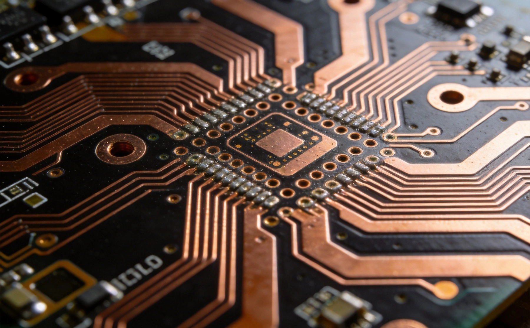
HDI stands for High Density Interconnect. An Hdi Pcb is a Printed Circuit Board that features a higher wiring density per unit area compared to traditional circuit boards. This is achieved through advanced Microvia Technology, which allows for smaller via sizes and tighter trace spacing.
The International Printed Circuit Committee (IPC) defines HDI PCBs as boards with one or more of the following characteristics:
When we talk about HDI in PCB, we're really talking about Miniaturization. Every smartphone, tablet, and wearable device on the market today relies on HDI Pcb Technology to pack complex functionality into increasingly compact form factors. Our manufacturing facilities in Shenzhen have produced millions of HDI boards for clients worldwide, and we've seen firsthand how this technology transforms product possibilities.
Not all HDI PCBs are created equal. The industry has developed several standard configurations to meet different performance and cost requirements. Understanding these types helps you make better decisions when sourcing from an HDI PCB manufacturer.
This is the most basic HDI structure, featuring one layer of high density interconnects on one or both sides of the core. The "1-N-1" designation means one build-up layer on each side of the core (N). It's a cost-effective entry point into Hdi Technology.
With two build-up layers on each side of the core, 2-N-2 offers higher routing density. This configuration is common in mid-range smartphones and Automotive Electronics where space is at a premium but budget constraints exist.
For the most demanding applications, manufacturers can produce HDI PCBs with three or more build-up layers. These ultra-high density boards are found in flagship smartphones, advanced medical devices, and aerospace systems where every millimeter matters.
Any Layer HDI represents the pinnacle of HDI technology. In this configuration, all layers are interconnected using blind and Buried Vias, creating maximum design flexibility. Apple's iPhone series famously uses Any Layer HDI in their main logic boards—a testament to the technology's capability.
The manufacturing of HDI PCBs requires precision, experience, and state-of-the-art equipment. Here's a simplified overview of our standard Hdi Pcb Manufacturing process:
Everything starts with a high-quality core material, typically FR-4 or high-Tg materials for improved reliability. The core is drilled with through-holes and any required buried vias using precision CNC drilling or Laser Drilling systems.
After drilling, we perform desmear treatment to remove any resin smear left on hole walls. This is followed by electroless copper deposition to create a conductive seed layer for subsequent plating operations.
This is where HDI magic happens. Build-up layers are added using Sequential Lamination. Each cycle involves:
The number of build-up cycles depends on your HDI Pcb Stackup requirements. Our facilities can handle up to 12+ build-up layers for the most complex designs.
After all layers are built up, we apply surface finishes (Hasl, Enig, Osp, or immersion tin) and perform electrical testing. Each HDI board undergoes 100% Aoi (Automated Optical Inspection) and flying probe testing to ensure zero defects.
The unique characteristics of high density interconnect PCBs make them ideal for a wide range of applications. Here are the sectors where we see the most demand:
Smartphones are the largest consumer of HDI PCBs. A typical flagship phone contains 8-12 layers of HDI routing, connecting processors, memory, RF components, and cameras in a footprint smaller than a credit card. Tablets, smartwatches, and wireless earbuds also rely heavily on HDI technology.
Modern vehicles contain dozens of ECUs (Electronic Control Units), infotainment systems, and advanced driver assistance systems (ADAS). HDI PCBs enable automakers to reduce weight and size while increasing functionality and reliability. Our automotive HDI boards meet Iatf 16949 quality standards.
From portable diagnostic equipment to implantable devices, medical electronics demand Miniaturization and reliability. HDI PCBs in medical applications include hearing aids, insulin pumps, patient monitors, and imaging equipment.
5G infrastructure and networking equipment use HDI technology for high-speed signal routing. The combination of Microvia Technology and Controlled Impedance design enables the data rates required for modern communications.
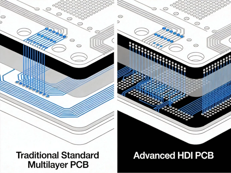
Choosing between HDI and standard multilayer PCBs depends on your specific requirements. Here's a practical comparison:
| Feature | Standard PCB | HDI PCB |
|---|---|---|
| Via Size | 0.3mm - 0.5mm | 0.1mm - 0.15mm (microvia) |
| Trace Width | 100μm - 200μm | 50μm - 75μm |
| Routing Density | Low to Medium | Medium to Ultra-High |
| Layer Count | 2-12 layers typical | 4-20+ layers typical |
| Typical Cost | Lower per unit | 20-50% higher than standard |
| Signal Integrity | Good for basic applications | Excellent for high-speed designs |
| Design Flexibility | Limited routing options | High routing density and flexibility |
In our experience, the decision usually comes down to three factors: board size constraints, Signal Integrity requirements, and budget. If your product needs to fit in a pocket or wearable form factor, HDI is almost always the right choice. If you have plenty of board space and simpler requirements, standard PCBs may be more cost-effective.
Working with the right HDI PCB manufacturer in China can make or break your product development. Based on years of serving global clients, here are the key factors we recommend evaluating:
Ask potential suppliers about their equipment and process capabilities. Key questions include:
Reliable HDI PCB manufacturers should hold relevant certifications including Iso 9001, Iso 14001, and Ul Certification. For automotive applications, Iatf 16949 is essential. Medical and aerospace suppliers may need additional qualifications.
The best manufacturers don't just take orders—they partner with you on design. Look for suppliers who offer:
HDI manufacturing is technically demanding. Ask about their experience with your specific application type. Have they produced boards for smartphones, automotive, medical, or other sectors relevant to your needs?
Current HDI technology allows for Microvias as small as 0.1mm (100μm) in diameter using laser drilling. Some advanced manufacturers can achieve 0.075mm or even smaller, though production yields decrease significantly at these extremes.
HDI PCBs typically cost 20-50% more than equivalent standard multilayer boards. The higher cost comes from specialized equipment, tighter process controls, and lower production yields. However, for space-constrained applications, HDI often reduces overall system cost by eliminating the need for additional boards or connectors.
Standard HDI PCB lead times range from 10-15 business days for production quantities. Complex Any Layer HDI boards may require 20-25 days. Expedited services are usually available for an additional fee.
Not always. While HDI offers superior density, standard PCBs may still be preferable for large, simple boards, high-power applications requiring thick copper, or cost-sensitive products with adequate space. The choice depends on your specific requirements.
Blind vias connect an outer layer to one or more inner layers without going through the entire board. Buried vias connect only inner layers and are not visible from the outside. Both are key enablers of HDI technology, allowing for more efficient routing and higher density.
HDI PCB technology represents a critical enabler for modern electronics miniaturization. From the smartphone in your pocket to the advanced medical devices saving lives, high density interconnect PCBs are everywhere.
Understanding the basics of HDI—the types available, manufacturing processes, applications, and how to select the right manufacturer—gives you a significant advantage when developing your next product. Whether you're designing a wearable device, automotive system, or IoT product, HDI may be the key to achieving your size and performance goals.
As an experienced China Hdi Pcb Manufacturer, we're here to help you navigate your HDI journey. Our engineering team has supported hundreds of clients in bringing their innovative products to market, and we'd be happy to discuss your specific requirements.
Ready to explore HDI technology for your next project? Contact our engineering team today for a free Dfm review and quote. We'll help you determine if HDI is right for your application and provide transparent pricing with no hidden costs.
How to Choose the Best China HDI PCB Manufacturer in 2026June/08/2026
Why Choose a China HDI PCB Manufacturer for Your Project?May/13/2026
The Future of PCB Manufacturing in China: Trends for 2026 and BeyondMay/19/2026
What is the Minimum Trace Width for HDI PCBs?July/17/2026
The Ultimate Guide to HDI PCB Technology You Need to KnowJune/02/2026
Top 5 Applications of HDI PCBs in Modern ElectronicsMay/13/2026
HDI PCB Manufacturing Process: Step-by-Step ExplanationMay/13/2026
HDI PCB vs Standard PCB: Key Differences ExplainedMay/13/2026