Open Nav

China has been the undisputed leader in global Pcb Manufacturing for decades, producing over half of the world's printed circuit boards. From the earliest days of simple single-sided boards to today's ultra-dense multi-layer interconnect structures, Chinese Manufacturers have continuously evolved to meet the ever-increasing demands of the electronics industry. But the landscape is shifting. New technologies, geopolitical dynamics, environmental pressures, and the relentless march of Miniaturization are fundamentally reshaping what it means to be a PCB manufacturer in China.
As we move through 2026 and look toward the next decade, the Chinese PCB industry stands at a crossroads. Labor costs have risen significantly over the past twenty years, narrowing the cost advantage that once made China the default choice for manufacturing. Meanwhile, competitors in Southeast Asia—Vietnam, Thailand, Malaysia, and India—are ramping up their capabilities and attracting attention from brands seeking to diversify their supply chains. Yet China retains overwhelming advantages in infrastructure, supply chain density, engineering talent, and manufacturing ecosystem depth that cannot be easily replicated elsewhere.
This article explores the defining trends shaping the future of Pcb Manufacturing in China. We will examine how advanced packaging technologies, artificial intelligence and Industry 4.0 integration, sustainability imperatives, geopolitical considerations, and emerging applications are driving transformation across the industry. Understanding these trends is essential for electronics designers, procurement professionals, and industry observers who want to anticipate changes in the global supply chain and make informed decisions about where and how their PCBs will be made.
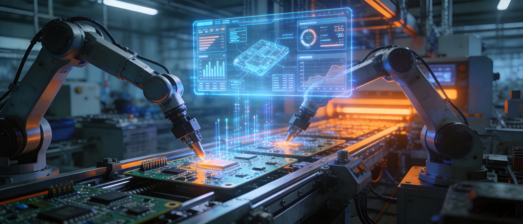
Before looking forward, it is worth understanding where the Chinese PCB industry stands today. China produces an estimated 55-60% of global PCB output by value, with over 2,000 PCB manufacturers operating within its borders. The industry spans a vast spectrum—from small, low-technology shops producing simple boards for consumer goods to ultra-advanced facilities capable of manufacturing 30+ layer boards, HDI (High Density Interconnect) structures, and advanced substrates for the most sophisticated semiconductor packages.
The industry is concentrated in several key regions:
The top Chinese PCB manufacturers have invested heavily in advanced capabilities, positioning themselves to serve the most demanding applications. Companies like Tripod Technology, HannStar Board, and Wus Printed Circuit have built facilities rivaling the best in Japan, Taiwan, or South Korea. Yet the industry as a whole remains highly fragmented, with thousands of smaller manufacturers competing on price for standard products.
The most significant transformation in Chinese PCB manufacturing is the rapid push toward advanced packaging technologies. For decades, Moore's Law drove semiconductor progress—transistors got smaller, chips got more powerful, and PCB manufacturers simply had to keep pace with the I/O density demands of increasingly powerful processors. But as traditional transistor scaling approaches physical limits, the industry has shifted to a new paradigm: packaging innovation.
Advanced packaging technologies—including chiplets, 2.5D interposers, 3D stacking, embedded die, and panel-level packaging—are redefining how semiconductors connect to each other and to the outside world. These technologies require equally advanced substrates and interposers that blur the line between semiconductor packaging and PCB manufacturing.
The chiplet movement—breaking large monolithic chips into smaller, specialized dies that are packaged together—is accelerating across the semiconductor industry. AMD, Intel, and others have embraced chiplet architectures for their performance and cost advantages. This approach demands sophisticated substrate technologies capable of connecting multiple dies with high-bandwidth, low-latency interconnects.
Chinese substrate manufacturers are investing heavily in this space. ABF (Ajinomoto Build-up Film) substrate production is expanding, with several Chinese companies building new facilities to compete with established Japanese and Korean suppliers. These substrates—featuring fine-line circuitry, micro-vias, and complex layer structures—are among the most challenging PCBs to manufacture and represent the high end of the industry's technological frontier.
Embedding active semiconductor dies inside the PCB substrate—rather than mounting them on the surface—is an emerging technology that enables unprecedented Miniaturization and performance. By eliminating the distance between the die and the circuit, embedded die technologies dramatically reduce signal latency and power consumption, making them ideal for high-performance computing, 5G communications, and advanced medical devices.
Panel-level packaging (PLP)—processing semiconductor packages on large rectangular panels rather than individual substrates—is another frontier. PLP offers significant cost advantages through economies of scale and the ability to package many more units simultaneously. Chinese Manufacturers are actively developing PLP capabilities, positioning themselves to serve the next generation of semiconductor packaging.
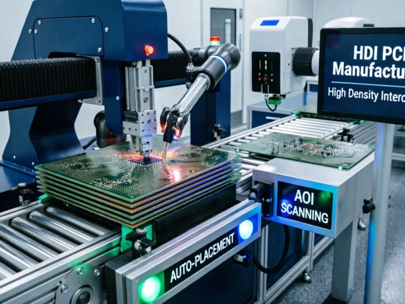
High Density Interconnect (HDI) boards with micro-vias, blind and Buried Vias, and fine-line circuitry have become essential for smartphones, tablets, and other compact electronics. The most advanced HDI boards—known as Any-layer Hdi—allow vias to connect any combination of layers, enabling extremely high interconnect density.
Chinese manufacturers have rapidly advanced their HDI capabilities. What was once the exclusive domain of Japanese and Taiwanese suppliers is now within reach of leading Chinese manufacturers. The competition has intensified, driving innovation and pushing the boundaries of what is achievable at increasingly competitive price points.
The fourth industrial revolution—characterized by the integration of digital technologies, data analytics, and automation into manufacturing—is transforming Chinese PCB factories. Artificial intelligence, machine learning, the Internet of Things (IoT), and digital twins are moving from buzzwords to operational realities on the factory floor.
AI is being deployed across the PCB manufacturing workflow to improve quality, efficiency, and predictability. In the drilling process, for example, AI algorithms analyze drill bit wear patterns, board characteristics, and historical data to optimize drilling parameters in real time, extending drill life and reducing breakage. In plating processes, AI controls chemical concentrations and current densities to maintain consistent quality across production runs.
Visual inspection—long a bottleneck in Quality Control—is being transformed by AI-powered Automated Optical Inspection (Aoi) and X-ray Inspection systems. Deep learning models trained on millions of images can now detect subtle defects that might escape human inspectors or rule-based automated systems. These systems continuously improve as they process more boards, learning from every defect detected.
Predictive maintenance—using sensor data and analytics to anticipate equipment failures before they occur—is reducing unplanned downtime in Chinese PCB factories. Vibration sensors on drilling spindles, temperature monitors on reflow ovens, and current sensors on plating lines all feed data into predictive models that flag anomalies before they cause quality problems or equipment failures.
Digital twins—virtual replicas of physical production systems—are enabling manufacturers to simulate process changes, optimize parameters, and troubleshoot issues without interrupting actual production. A manufacturer planning to introduce a new board design can create a digital twin of the production process, identify potential issues, and optimize parameters before the first physical board is produced.
The ultimate vision is the fully integrated smart factory, where every machine, process, and system is connected and coordinated through a central nervous system. In such facilities, production scheduling optimizes itself based on order priorities, equipment status, material availability, and energy costs. Quality data flows automatically from inspection systems to process controls, enabling real-time adjustment. And management has complete visibility into operations through dashboards powered by real-time data analytics.
Leading Chinese PCB manufacturers are well along this journey. Companies like ShenZhen Fastprint Circuit Tech and others have invested heavily in MES (Manufacturing Execution Systems), ERP integration, and shop-floor automation. The gap between the most advanced Chinese manufacturers and their global competitors has largely closed—and in some areas, Chinese factories lead the world in digital sophistication.
Environmental sustainability has moved from a peripheral concern to a core strategic priority for Chinese PCB manufacturers. Regulatory pressure, customer requirements, and genuine corporate responsibility are driving fundamental changes in how PCBs are made.
PCB manufacturing is water-intensive, particularly in the plating and cleaning processes that require large volumes of ultrapure water. Chinese manufacturers are responding with aggressive water conservation programs. Advanced wastewater treatment and recycling systems can now recover and reuse 70-90% of process water, dramatically reducing freshwater consumption.
Zero-liquid-discharge (ZLD) systems—which eliminate all wastewater discharge through evaporation, crystallization, and advanced treatment—are being adopted by the most progressive manufacturers. While ZLD systems require significant capital investment, they eliminate environmental risk and position manufacturers to meet increasingly stringent discharge regulations.
The transition to lead-free soldering—a response to RoHS and similar regulations—demonstrated how regulatory pressure can drive industry-wide change. Building on that foundation, manufacturers are now tackling broader chemical management challenges. Reductions in halogenated compounds, elimination of specific chemicals of concern, and selection of greener alternatives for cleaning and surface treatment are all underway.
The trend toward halogen-free PCBs—driven by fire safety and environmental concerns—is accelerating. While halogen-free materials present manufacturing challenges, they offer improved fire safety performance and reduced environmental impact, making them increasingly attractive for consumer electronics, automotive, and other applications.
As global attention to climate change intensifies, PCB manufacturers face growing pressure to measure and reduce their carbon footprints. Leading Chinese manufacturers are responding with energy efficiency improvements, renewable energy procurement, and carbon offset programs.
Solar panel installations on factory rooftops are common among larger manufacturers. Led Lighting, variable-frequency drives on motors, and advanced reflow oven designs are reducing energy consumption per unit of production. Some manufacturers are exploring partnerships with renewable energy providers to power their operations with wind or solar electricity.
The concept of extended producer responsibility (EPR)—whereby manufacturers take responsibility for the end-of-life management of their products—is gaining traction. While EPR is more commonly associated with consumer products, the electronics industry is beginning to grapple with the implications for components like PCBs.
Design for recyclability—considering how boards will be disassembled and materials recovered at end of life—is emerging as a consideration for forward-thinking manufacturers. While the technical challenges are significant (mixed materials, complex laminates, and attached components make recycling difficult), the industry is beginning to explore approaches that could facilitate circular economy principles.
Geopolitical tensions—particularly between the United States and China—have introduced new uncertainties into the global Electronics Supply Chain. Tariffs, export controls, and concerns about Supply Chain Resilience are driving companies to re-evaluate their manufacturing footprints.
Many electronics companies have adopted "China Plus One" strategies—maintaining manufacturing capabilities in China while establishing alternative production bases in other countries. Vietnam, Thailand, Malaysia, and Indonesia have attracted significant investment as companies seek to reduce their exposure to single-country risk.
For PCB manufacturing specifically, the China Plus One dynamic is more nuanced. While some lower-technology Pcb Production is migrating to Southeast Asia, the concentration of advanced manufacturing capabilities, supplier ecosystems, and engineering talent in China remains difficult to replicate elsewhere. Most companies seeking high-technology PCBs—HDI, advanced substrates, Flex Circuits—find that China's ecosystem advantage is decisive.
China's massive domestic electronics market—driven by smartphones, electric vehicles, renewable energy systems, industrial automation, and consumer electronics—provides a powerful tailwind for domestic PCB manufacturers. The Chinese government's "Made in China 2025" initiative and subsequent policies have actively promoted the development of domestic capabilities in advanced manufacturing, including PCBs and Electronic Manufacturing services (EMS).
This policy support has accelerated investment in advanced PCB capabilities, with government-backed research programs and subsidies helping manufacturers upgrade their technologies. The combination of policy support and domestic market demand is positioning Chinese manufacturers to lead in emerging applications like electric vehicle electronics, 5G infrastructure, and industrial IoT.
US export controls targeting advanced semiconductor technologies have created new challenges for Chinese manufacturers. Restrictions on advanced equipment, software, and materials have raised concerns about the long-term technological trajectory of Chinese PCB and semiconductor industries.
Chinese manufacturers are responding with accelerated domestic development programs, seeking to build capabilities in equipment and materials that were previously imported. While complete self-sufficiency is unrealistic in the near term, the momentum toward domestic supply chain development is significant. The outcome of this technology competition will have profound implications for the global electronics industry.
Emerging applications across multiple industries are creating new demands on PCB manufacturers, driving innovation and specialization.
The rapid growth of electric vehicles represents a massive opportunity—and a significant technical challenge—for PCB manufacturers. Electric vehicles require sophisticated battery management systems (BMS), Power Electronics (inverters, converters, chargers), motor controllers, and autonomous driving electronics. These applications demand PCBs with unique characteristics:
Chinese manufacturers are investing heavily in Automotive Pcb capabilities, seeking to serve both domestic EV manufacturers and the global automotive industry. Several Chinese companies have obtained automotive quality certifications (Iatf 16949) and are supplying PCBs to major automotive OEMs and Tier 1 suppliers.
The rollout of 5G networks—featuring higher frequencies, wider bandwidths, and massive antenna systems—is driving demand for specialized PCBs. 5G base stations, smartphones, and IoT devices require boards with:
Chinese PCB manufacturers have positioned themselves to serve the 5G market, developing capabilities in high-frequency materials, thermal management, and ultra-High-density Interconnect. The scale of 5G deployment in China—already the world's largest 5G market—provides a significant domestic demand driver.
The proliferation of IoT devices—smart home products, industrial sensors, wearable electronics, and connected health devices—is creating demand for PCBs that are small, inexpensive, and often flexible. Flexible and rigid-flex PCBs are enabling new product form factors that would be impossible with rigid boards alone.
Wearable electronics—fitness trackers, smart watches, health monitors—require ultra-miniaturized boards that conform to curved surfaces, integrate sensors and displays, and operate within tight power budgets. Chinese manufacturers are developing specialized capabilities in flexible circuits, stretchable substrates, and ultra-miniaturized assembly to serve this growing market.
Medical electronics—from diagnostic equipment to implantable devices—represent a high-value, high-growth segment for PCB manufacturers. Medical devices demand:
Chinese manufacturers are pursuing Medical Pcb capabilities, with several obtaining Iso 13485 certification and supplying boards for medical devices. The aging populations in China and globally are driving sustained growth in medical electronics, creating long-term opportunities for manufacturers that can meet stringent requirements.
The transformation of Chinese PCB manufacturing extends to its workforce. Automation and digitalization are changing the skills required, the nature of manufacturing jobs, and the competitive dynamics of the labor market.
Rapid automation in Chinese PCB factories is displacing some traditional manufacturing jobs while creating new roles in robotics maintenance, automation programming, and digital systems management. The labor intensity of PCB manufacturing has decreased significantly—some highly automated facilities now employ fewer than 50 people per 1,000 square meters of production space.
This shift is changing the demographic profile of the PCB workforce. Demand for skilled technicians, automation engineers, and data analysts is growing, while demand for basic assembly workers is declining. Manufacturers are investing in workforce development programs to upskill their existing employees and attract new talent with relevant technical backgrounds.
The depth of engineering talent in China remains one of its most significant competitive advantages. Chinese universities graduate large numbers of electrical, mechanical, and chemical engineers each year. Combined with experienced engineers who have built expertise through decades of manufacturing at scale, this talent pool enables rapid innovation and continuous process improvement.
As Chinese PCB manufacturers move up the value chain—competing in advanced packaging, HDI, and specialized substrates—engineering talent becomes even more critical. The ability to develop new processes, solve complex technical problems, and continuously improve quality depends on attracting, developing, and retaining skilled engineers.
Rising labor costs in coastal China are driving some manufacturing inland and to lower-cost regions. Cities in central and western China—Zhengzhou, Wuhan, Chongqing—are emerging as new manufacturing centers, offering lower labor costs while benefiting from improved infrastructure and logistics networks.
For PCB manufacturers, the calculus is more complex. While labor costs matter, the ecosystem advantages of the Pearl River Delta and Yangtze River Delta—concentrated supplier networks, established logistics, and deep engineering talent—often outweigh marginal labor cost differences, particularly for high-technology products.
The Chinese PCB industry is undergoing significant consolidation. While thousands of small manufacturers continue to operate, the industry is concentrating as larger, more capital-efficient companies acquire smaller competitors and expand their capabilities.
Advanced PCB manufacturing requires substantial capital investment. A state-of-the-art HDI production line can cost hundreds of millions of dollars to build and equip. This capital intensity favors larger companies that can spread investment costs across higher volumes and access financing on favorable terms.
Economies of scale also improve operational efficiency. Larger manufacturers can invest in automation, process optimization, and quality systems that would be uneconomical for smaller operations. These scale advantages translate into lower costs, better quality, and superior customer service—all of which compound competitive advantages over time.
Leading Chinese PCB manufacturers are pursuing strategic acquisitions to expand their capabilities and customer bases. Vertical integration—acquiring upstream suppliers of laminates, chemicals, or equipment—is one common strategy. Horizontal integration—acquiring competitors with complementary capabilities or geographic reach—is another.
Publicly traded PCB companies have particular advantages in pursuing M&A strategies, with access to capital markets and established corporate governance structures. Several major acquisitions have reshaped the competitive landscape in recent years, and the consolidation trend is expected to continue.
Despite consolidation at the high end, the Chinese PCB industry retains a long tail of small manufacturers serving commodity markets. These companies—often family-owned or privately held—compete on price for standard, low-complexity PCBs. Competition in this segment is intense, and margins are thin.
The future of small manufacturers in China is uncertain. Rising costs, environmental regulations, and competitive pressure from larger players are squeezing margins. Some will continue to survive serving niche markets or local customers, while others will exit the industry or be acquired. The survival of small manufacturers will depend on finding defensible niches—whether in specialized products, Rapid Prototyping, or highly customized small-batch production.
The way customers interact with PCB manufacturers is changing, driven by digital platforms, online marketplaces, and rising expectations for transparency and convenience.
Online platforms that enable instant PCB quotations, design file uploads, and order tracking are transforming the customer experience. Companies have developed sophisticated algorithms that can analyze uploaded Gerber files, assess manufacturing complexity, and generate accurate quotes in seconds—replacing the days or weeks that traditional quotation processes once required.
These platforms serve both prototype and small-batch customers who need rapid turnaround as well as larger customers seeking convenient access to standard products. By automating routine tasks and enabling self-service, digital platforms reduce costs for manufacturers while improving convenience for customers.
Customers increasingly expect transparency into their orders—knowing where their boards are in the production process, when they will ship, and what quality data supports the finished product. Manufacturers are responding with improved ERP and MES integration that provides real-time order tracking, automated status updates, and access to quality documentation.
Blockchain technology is being explored for supply chain traceability, enabling customers to verify the origin and authenticity of materials and components in their PCBs. While adoption remains limited, the underlying trend toward greater transparency is clear.
The best PCB manufacturers are evolving from transactional suppliers to strategic partners that help customers optimize their designs for manufacturability, cost, and performance. Online Dfm tools that provide instant design feedback, downloadable CAD libraries with manufacturing-compatible components, and collaborative engineering platforms are making it easier for customers to design PCBs that work well with manufacturing processes.
For electronics companies that rely on PCBs, the trends shaping the Chinese industry have important strategic implications.
While China will remain the world's dominant PCB manufacturer for the foreseeable future, the rationale for supply chain diversification has strengthened. Companies should evaluate whether their current supplier concentration is appropriate for their risk tolerance and business requirements.
For companies that choose to diversify, the approach should be strategic rather than reflexive. Identify which products or applications truly benefit from diversification, evaluate alternative manufacturing locations objectively, and develop relationships with backup suppliers before they are urgently needed.
As PCB complexity increases, the choice of manufacturing partner becomes more consequential. Companies should seek partnerships with manufacturers that are investing in advanced capabilities—not just today, but with credible plans for continued technological advancement.
Look for manufacturers that actively engage in Dfm discussions, share process capability data, and invest in quality systems. The best manufacturing partnerships are collaborative, with both parties working together to optimize designs, reduce costs, and improve quality over time.
In an industry undergoing rapid change, long-term relationships with capable manufacturers become more valuable, not less. Manufacturers that know your products, understand your quality requirements, and have invested in your success are better positioned to support your evolving needs.
Invest in building relationships with key supplier contacts. Share your product roadmap so manufacturers can plan their capability development. Treat manufacturing partners as strategic assets to be developed and maintained rather than transactional suppliers to be squeezed.
Yes, China is expected to remain the world's largest PCB manufacturer through 2030 and beyond. Despite rising labor costs and geopolitical pressures, China's overwhelming advantages in infrastructure, supply chain density, manufacturing ecosystem depth, and engineering talent are not easily replicated elsewhere. While some lower-technology production may migrate to lower-cost regions, China's dominance in advanced PCB manufacturing will likely persist.
The most significant trends include advanced packaging technologies (chiplets, substrates, embedded die), AI and Industry 4.0 integration, sustainability and environmental compliance, HDI and any-layer technology advancement, and capabilities development for specific applications like electric vehicles, 5G, and medical electronics.
Yes. Leading Chinese PCB manufacturers have achieved quality levels that match or exceed the best manufacturers anywhere in the world. Many hold Iso 9001, Iatf 16949 (automotive), ISO 13485 (medical), and other quality certifications. For demanding applications like automotive, medical, or aerospace, it is important to carefully vet manufacturers' specific capabilities and track records.
Trade tensions have introduced uncertainties into the global Pcb Supply Chain, including tariffs on certain products and restrictions on advanced technology transfers. Many companies have responded by diversifying their supplier base, while Chinese manufacturers have accelerated domestic capability development. The long-term impact depends on the evolution of trade policies, which remain uncertain.
PCB manufacturing wages in China have risen significantly over the past two decades and are expected to continue increasing, though at a slower pace. This trend is driving automation investment and shifting the industry toward higher-value, more capital-intensive production. However, China's absolute labor cost advantage—considering productivity levels—remains competitive for most PCB categories.
Chinese PCB manufacturers are investing heavily in environmental compliance, including wastewater treatment and recycling, chemical management systems, energy efficiency improvements, and adoption of greener materials. Leading manufacturers have implemented Iso 14001 environmental management systems and pursue continuous improvement in their environmental performance.
Key growth drivers include electric vehicles and Automotive Electronics, 5G communications infrastructure and devices, Internet of Things devices and wearables, artificial intelligence and data center hardware, medical electronics, and industrial automation. These applications demand increasingly advanced PCB technologies, driving capability development across the industry.
Finding a reliable manufacturer requires careful evaluation. Look for appropriate quality certifications, request samples and references, verify manufacturing capabilities match your requirements, assess communication and responsiveness, and consider starting with a small order to evaluate the relationship before committing to larger volumes. Industry trade shows and directories can help identify potential partners.
The future of PCB manufacturing in China is being written by powerful forces: advanced packaging technologies that blur the boundaries between semiconductors and PCBs, artificial intelligence and Industry 4.0 that are transforming factory operations, sustainability imperatives that demand environmental responsibility, geopolitical dynamics that reshape supply chains, and emerging applications that push the boundaries of what PCBs must do.
For all the change, China's fundamental strengths remain formidable. The density of its manufacturing ecosystem, the depth of its engineering talent, the scale of its domestic market, and the investment capacity of its leading companies create advantages that will persist for decades. Chinese manufacturers that successfully navigate the technology frontier will be essential partners for electronics companies worldwide.
The manufacturers that will thrive are those that embrace advanced technologies, invest in sustainability, develop deep engineering capabilities, and build lasting customer relationships. The era of competing simply on cost is ending. The era of competing on technology, quality, and innovation is just beginning.
For electronics designers, procurement professionals, and industry observers, understanding these trends is not just an intellectual exercise—it is a practical necessity. The decisions you make today about manufacturing partners, supply chain strategies, and technology choices will determine your competitiveness in an industry that never stands still.
The future of PCB manufacturing in China is bright, complex, and full of opportunity for those who understand it well.
What is HDI PCB? A Complete Guide from China HDI PCB ManufacturerMay/13/2026
HDI PCB Manufacturing Process: Step-by-Step ExplanationMay/13/2026
Top 5 Applications of HDI PCBs in Modern ElectronicsMay/13/2026
The Ultimate Guide to HDI PCB Technology You Need to KnowJune/02/2026
What is the Minimum Trace Width for HDI PCBs?July/17/2026
Understanding HDI PCB Technology: A Comprehensive Guide for BeginnersMay/13/2026
Why Choose a China HDI PCB Manufacturer for Your Project?May/13/2026
How to Choose the Best China HDI PCB Manufacturer in 2026June/08/2026