Open Nav

When your product design demands Miniaturization, performance, and reliability, choosing between Hdi Pcb vs standard PCB becomes one of the most critical decisions in your development process. Many engineers and product managers find themselves asking: what's the real difference, and which one does my project actually need?
Having manufactured millions of both types of boards for clients across the globe, we understand the nuances that go beyond textbook definitions. In this comprehensive guide, we'll walk you through every meaningful difference between HDI and standard PCBs, so you can make an informed decision backed by real manufacturing experience.
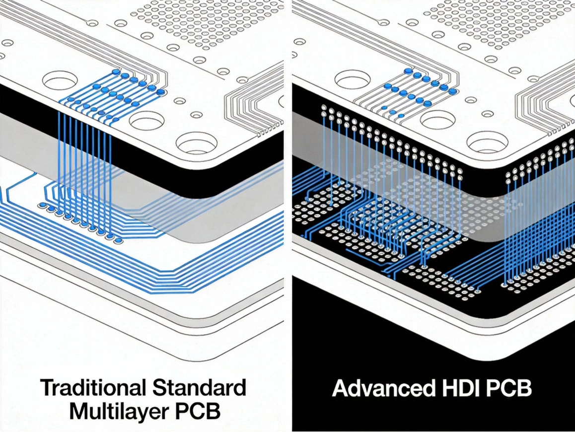
Standard PCBs, also called conventional or traditional multilayer PCBs, have been the backbone of Electronics Manufacturing for decades. These boards use through-hole vias that connect all layers from top to bottom, with trace widths and spacing typically ranging from 100μm to 200μm.
The Manufacturing Process for standard PCBs is well-established and straightforward. Drill holes, plate through-holes, apply copper patterns, and finish with surface treatment. Simple, reliable, and cost-effective for designs that have adequate space.
HDI stands for High Density Interconnect. HDI PCBs take Miniaturization to the next level through advanced features like Microvias (0.1mm or smaller), buried and Blind Vias, and finer trace geometries down to 50μm or less. The build-up layer technology allows for dramatically higher wiring density in the same or smaller board area.
Think of it this way: if standard PCBs are like city streets with traffic lights at every intersection, HDI PCBs are like highways with multiple lanes and express routes. Both get the job done, but one handles complexity far more efficiently.
The most fundamental distinction between HDI and standard PCBs lies in their via technology. In standard PCBs, through-hole vias connect every single layer from surface to surface. This means even if you only need to connect layer 2 to layer 3, that connection still passes through all layers.
HDI PCBs introduce two game-changing via types that solve this inefficiency:
In our production facilities, we've seen designs that reduced their board size by 40% just by switching from standard Pcb Technology to HDI, primarily thanks to these via technologies. The routing freedom they provide is transformative.
Standard PCBs typically follow a simple symmetric or asymmetric layer stackup where each layer is connected through the entire board. Adding more functionality usually means adding more layers and more board area.
Hdi Pcb stackups use sequential build-up layers. Instead of drilling through everything, each build-up layer adds routing density where it's needed most. The result is that an 8-layer HDI board can often outperform a 12-layer standard PCB in routing efficiency while taking up less space.
Common HDI structures include:
Both PCB types can use similar base materials, but HDI manufacturing often benefits from higher-performance substrates. Low-Dk, low-Df materials for high-speed signals are easier to implement in HDI stackups due to the shorter via lengths and Controlled Impedance paths.
Here's where Hdi Technology truly shines for modern applications. The shorter via lengths in HDI boards mean reduced stub effects in high-speed signal paths. Microvias behave more like ideal connections at high frequencies compared to long through-hole stubs.
For applications like 5G communications, advanced driver assistance systems, and high-speed computing interfaces (PCIe 5.0, DDR5, USB4), the Signal Integrity advantages of HDI can be the difference between meeting and failing compliance testing. We've helped numerous clients pass EMI and Signal Integrity tests by migrating to HDI designs where standard PCBs simply couldn't meet the requirements.
Standard PCBs have the advantage when it comes to power distribution in high-current applications. The ability to use thicker copper and larger planes for power delivery is straightforward in standard constructions. HDI boards can handle power distribution too, but may require more careful planning for high-current designs.
If your design involves power MOSFETs, motor controllers, or high-power RF amplifiers, standard PCB construction might offer more flexibility for power plane implementation. However, for most digital and mixed-signal designs, HDI handles power distribution adequately.
Thermal Dissipation presents different challenges for each technology. Standard PCBs allow for larger thermal vias and direct copper pours that extend across multiple layers without interruption. HDI PCBs require more strategic thermal routing since blind and buried vias create boundaries in the layer stackup.
That said, the higher density of HDI means heat sources can be placed closer together, and thermal interface materials can be applied more effectively. Many thermal engineers we've worked with have found creative solutions in HDI designs that actually outperform standard boards in compact thermal packages.
Let's address the elephant in the room: HDI PCBs cost more than standard PCBs. Understanding why and whether the premium is justified is crucial for your design decisions.
Several factors contribute to higher HDI manufacturing costs:
The HDI premium is absolutely worth it when:
Save your budget and use standard PCBs when:
Standard Pcb Design rules are well-understood and supported across all EDA tools. Design teams can typically achieve good results with moderate attention to detail.
HDI design requires more careful attention to:
We always recommend engaging your manufacturer early in the design process for HDI projects. A Dfm review before PCB Fabrication can save weeks of debugging and thousands of dollars in respins.
Standard PCB Dfm focuses on manufacturability at the individual layer level. HDI DFM must consider the entire build-up sequence and how each step affects subsequent layers.
Some common HDI DFM considerations include:
Consider a flagship smartphone mainboard. It might be a 10-layer Any Layer HDI board measuring 50mm x 80mm, containing a 1,000+ pin application processor, multiple DRAM packages, RF components, and dozens of discrete components—all densely packed.
Compare this to an industrial motor controller board. It might be a 4-layer standard PCB measuring 150mm x 200mm, with larger components, wider spacing, and more straightforward routing. Both are valid PCBs, but they serve completely different design philosophies.
A smartwatch PCB needs to fit in a few square centimeters while handling Bluetooth, Wi-Fi, sensors, display, and battery management. HDI is essentially mandatory for this form factor.
An automotive body control module has more space available, must meet strict automotive temperature and vibration requirements, and typically uses standard or HDI construction depending on the specific BCM complexity. Many automotive ECUs successfully use 2-N-2 HDI for the right balance of density and cost.
Here's a practical framework we use with clients when recommending Pcb Technology:
| Specification | Standard PCB | HDI PCB |
|---|---|---|
| Minimum Via Size | 0.3mm mechanical drill | 0.1mm laser drill (microvia) |
| Minimum Trace/Space | 100μm - 200μm | 50μm - 75μm |
| Via Types | Through-hole only | Through-hole, blind, buried, microvia |
| Typical Layer Count | 2-12 layers | 4-20+ layers |
| Routing Density | Low to Medium | Medium to Ultra-High |
| Board Size Reduction | Baseline | 20-50% smaller possible |
| Signal Integrity | Good for standard speeds | Excellent for high-speed designs |
| Typical Lead Time | 5-10 business days | 10-20 business days |
| Cost Premium | Baseline | 20-50% higher |
| Design Complexity | Moderate | High |
| Manufacturing Complexity | Standard | Advanced |
| High-Speed Performance | Limited | Superior |
Technically yes, but it's usually not cost-effective. HDI makes the most economic sense when board size is constrained. For large boards with plenty of routing space, the manufacturing premium doesn't deliver proportional value. We recommend HDI when board area reduction of 20% or more would benefit your product.
No, when properly designed and manufactured, HDI PCBs are equally reliable. In fact, for high-reliability applications like automotive and medical, HDI can offer advantages due to fewer plated through-holes (which are potential failure points) and better Thermal Management in compact packages. All our HDI boards undergo rigorous thermal cycling and microsection analysis to verify reliability.
HDI manufacturing has higher setup costs, so most manufacturers have higher minimum order quantities compared to standard PCBs. We typically see minimums ranging from 5-20 panels depending on the HDI complexity. Prototype quantities are possible but carry higher per-unit costs. For quick-turn prototypes, some shops offer reduced HDI options or rigid-flex alternatives.
A good test: if your standard Pcb Design would require more than 8-10 layers to route, or if your board area is constrained by more than 30% compared to a comfortable layout, Hdi Technology likely makes sense. Also consider whether you have high-pin-count BGA components (0.4mm pitch or finer) that would benefit from microvia escape routing.
Absolutely. Many complex designs use a standard PCB core with HDI build-up layers on specific areas. This hybrid approach targets HDI density where needed while controlling costs in less critical areas. Our engineering team regularly helps clients optimize such mixed-technology designs.
The HDI PCB vs standard PCB decision isn't about which technology is "better"—it's about which is right for your specific application. Both technologies have their place in modern electronics, and the best designs leverage each appropriately.
Standard PCBs offer proven reliability, straightforward design rules, and competitive pricing for applications with adequate space. HDI PCBs deliver unmatched density, superior signal integrity, and miniaturization capabilities for space-constrained and high-performance designs.
As an experienced China PCB Manufacturer, we've helped thousands of clients navigate this decision. Whether you ultimately choose HDI or standard PCB technology, the right choice should be driven by your product requirements, not by technology hype.
Need help determining which PCB technology is right for your design? Our engineering team offers free DFM consultations and can provide detailed cost comparisons for your specific application. Upload your design files today and let our experts guide your technology selection.
The Ultimate Guide to HDI PCB Technology You Need to KnowJune/02/2026
Why Choose a China HDI PCB Manufacturer for Your Project?May/13/2026
Understanding HDI PCB Technology: A Comprehensive Guide for BeginnersMay/13/2026
How to Choose the Best China HDI PCB Manufacturer in 2026June/08/2026
Top 5 Applications of HDI PCBs in Modern ElectronicsMay/13/2026

HDI PCB Manufacturing Process: Step-by-Step ExplanationMay/13/2026
What is the Minimum Trace Width for HDI PCBs?July/17/2026

The Future of PCB Manufacturing in China: Trends for 2026 and BeyondMay/19/2026