Open Nav

China has long been the world's manufacturing powerhouse, and nowhere is this more evident than in the production of printed circuit boards. Every smartphone, laptop, medical device, and automotive control system that you use likely contains PCBs that were designed, engineered, and manufactured with meticulous care in a facility somewhere in Guangdong, Jiangsu, Zhejiang, or Shanghai. But what actually happens inside these factories? What separates a world-class PCB manufacturer from an also-ran?
We invite you to put on a safety vest and hairnet, and follow us through the halls of our manufacturing facility. This behind-the-scenes tour will take you from the raw materials arriving at our loading docks to the finished boards being carefully packaged for shipment to customers on five continents. You will see the people, machines, and processes that transform simple fiberglass and copper into the nervous systems of the electronics that power our modern world.
Whether you are an electronics designer seeking a reliable manufacturing partner, a procurement professional evaluating suppliers, or simply curious about how the devices around you are made, this tour will give you a new appreciation for the craftsmanship and technology that goes into every PCB.
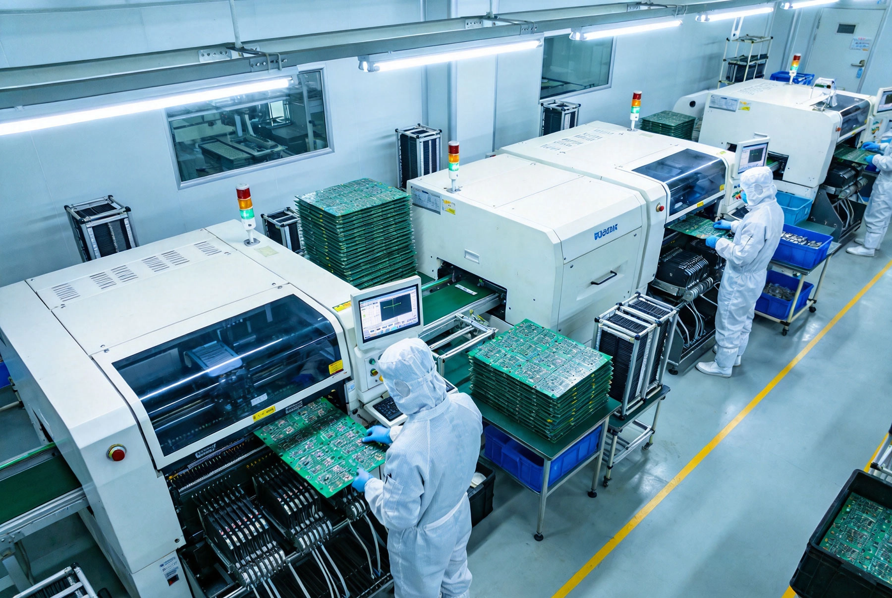
The first thing you notice when entering our facility is the level of organization. The factory floor is divided into clearly marked zones: incoming materials inspection, PCB production, Smt Assembly, testing and Quality Control, and shipping. Color-coded floor markings guide foot traffic, while distinct pathways are designated for raw materials entering and finished products leaving. This physical organization reflects a deeper commitment to process discipline that permeates everything we do.
Every visitor receives a safety briefing and is equipped with appropriate personal protective equipment (PPE). Electrostatic discharge (ESD) is the enemy of sensitive electronics, so everyone entering the assembly areas must wear ESD-safe footwear, wrist straps when handling boards, and anti-static smocks. These precautions are not just bureaucratic requirements—they are essential for protecting the products we make.
Temperature and humidity are controlled throughout the facility. Our assembly areas maintain 22-24°C and 40-60% relative humidity. Air filtration systems remove particulates down to ISO Class 7 standards in the most sensitive areas. This controlled environment ensures consistent manufacturing conditions and prevents moisture-related defects in finished boards.
Before any material touches our production lines, it undergoes rigorous incoming inspection. This is the first line of defense against defects—not just for our customers, but for our own efficiency. Catching problems at the source is always cheaper than catching them after value has been added.
Our primary raw material is PCB laminate—the fiberglass or composite substrate that forms the foundation of every board. We source laminates from approved suppliers who meet our exacting specifications for material properties, thickness consistency, and surface quality. Each incoming lot is tested for:
Substrates that do not meet our specifications are rejected and returned to the supplier. We maintain detailed quality records for every lot, enabling full traceability from finished product back to the original material certification.
For our Turnkey PCB Assembly services, we also receive and inspect electronic components. Our incoming inspection team verifies:
Components are stored in climate-controlled rooms with strict FIFO (first in, first out) inventory management. Moisture-sensitive devices (MSDs) are kept in dry cabinets until they are ready to be mounted on boards, at which point they undergo the standard floor life exposure before reflow.
The journey from raw laminate to a finished PCB involves multiple stages of processing. Each stage is carefully controlled, with inspection checkpoints at critical transitions.
Laminate sheets arrive in standard sizes (typically 4 feet by 4 feet or 4 feet by 5 feet). The first production step is to cut them into production panels sized appropriately for the specific board design. CNC cutting stations use precision saws or routers to cut panels with tight tolerances and clean edges.
Panel preparation also includes beveling edges for certain applications, adding tooling holes for automated handling, and creating breakaway tabs for panelized designs. We use advanced nesting software to maximize material utilization, reducing waste and lowering costs for our customers.
Drilling is one of the most critical operations in Pcb Manufacturing. The holes in a PCB serve multiple purposes: they provide pathways for through-hole component leads, they create vias connecting different layers in multi-layer boards, and they enable electrical testing access points.
Our facility operates computer-controlled drilling machines equipped with high-speed spindles and automatic tool changers. These machines can drill thousands of holes per minute with positional accuracy of ±0.025 mm. Drilling parameters are optimized based on hole size, board thickness, and laminate type to minimize hole wall roughness and prevent drill breakage.
A single multi-layer board may require dozens of different hole sizes, from 0.2 mm vias to 3.2 mm mounting holes. The drilling program sequences these in a way that minimizes tool changes and optimizes throughput while maintaining quality.
After drilling, boards undergo desmear and electroless copper plating processes. Desmear removes any resin smear left in the holes from the drilling process, while electroless copper deposits a thin conductive layer on the hole walls, preparing them for subsequent plating operations.
For double-sided and multi-layer boards, through-hole walls must be made electrically conductive. This is achieved through pattern plating—a process that adds copper only where needed, building up traces and plated-through-hole walls simultaneously.
The plating process involves:
For multi-layer boards, this process is repeated for each layer, with each layer being aligned to the previous one using precision registration holes and optical alignment systems. Layer-to-layer registration of ±0.05 mm is routinely achieved on our advanced equipment.
The exposed copper on a finished PCB must be protected from oxidation while remaining solderable for component assembly. We offer multiple surface finish options, each with different characteristics:
Our engineering team helps customers select the most appropriate surface finish based on their assembly requirements, storage conditions, and cost constraints.
Two final finishing steps add the visual and protective layers to the PCB:
Solder mask is the green (or other colored) coating that covers the PCB surface between traces and pads. It protects the copper from oxidation and prevents accidental solder bridges during assembly. We apply solder mask using screen printing or photo-imaging processes that achieve fine resolution and precise registration to the underlying circuitry.
Silkscreen legend (also called silk layer or nomenclature) adds the white text and symbols that identify component reference designators, test points, logos, and other markings. This is applied after solder mask and is also used to indicate orientations for polarized components, version numbers, and manufacturing date codes.
The final production step shapes the PCB to its designed dimensions and form factor. CNC routing machines use diamond-tipped tools to cut the board outline, create any complex shapes or cutouts, and separate panelized boards into individual units.
For boards with V-groove Panelization, a specialized V-cut machine scores the panel edges, leaving just enough material for panel integrity during assembly while allowing easy separation by the end user.
Once bare PCBs are completed, they move to our Smt Assembly area—the heart of our manufacturing operation. This is where electronic components are mounted onto the boards to create functional circuits.
The SMT assembly process begins with solder paste printing. As detailed in our companion guide on solder paste printing science, this critical step determines the foundation for every solder joint. Our factory operates a fleet of high-precision stencil printing systems equipped with:
Our SPI systems measure every deposit on critical boards, providing statistical process control data that allows us to detect and correct drift before it causes defects.
After paste printing, boards move to our pick-and-place lines. These automated assembly systems are the marvels of modern Electronics Manufacturing, capable of placing tens of thousands of components per hour with accuracy measured in hundredths of a millimeter.
Our facility features multiple placement lines with equipment from leading manufacturers including Fuji, Panasonic, and ASM. Each line includes:
Component placement programs are created using CAD data from our customers' design files. Our programming team uses advanced software to optimize placement sequences, feeder configurations, and head selections for maximum throughput and quality. Programs are verified against the original design data before being released to production.
After components are placed, the boards enter reflow ovens—the industrial furnaces that melt the solder paste and permanently attach components to the board. Our reflow lines use forced convection heating with multi-zone temperature control, enabling precise profiling for a wide range of board types and thermal masses.
Temperature profiling is performed for each new board design to ensure the reflow profile is optimized for the specific thermal requirements. Key parameters monitored include:
We use nitrogen atmosphere in some reflow chambers for sensitive applications, reducing oxidation and improving wetting for lead-free solders. Real-time thermal monitoring systems track every board through the reflow profile, flagging any that deviate from specifications.
For boards that include through-hole components—connectors, transformers, large electrolytic capacitors, or components requiring extra mechanical strength—we operate dedicated through-hole assembly lines with radial and axial insertion equipment.
Inserted components are secured using wave soldering, where the board is passed over a standing wave of molten solder. Selective soldering systems can also be used for boards with a mix of through-hole and surface mount components, allowing precise control over which joints are soldered and which are not.
After reflow, every board undergoes multiple inspection stages:
Automated Optical Inspection (Aoi) uses high-resolution cameras and sophisticated image processing algorithms to compare each board against a reference design. Aoi detects missing components, misplacements, tombstoning, solder bridging, insufficient solder, and a wide range of other defects. Our AOI systems are configured with custom inspection criteria optimized for each product.
X-ray Inspection is used for boards with hidden solder joints, particularly BGAs, QFNs, and other bottom-terminated components. X-ray imaging reveals the solder beneath the component, detecting issues like voiding, head-in-pillow defects, and insufficient wetting that optical systems cannot see.
In-Circuit Testing (ICT) applies electrical test signals to the board and verifies that each component and circuit node functions correctly. ICT can detect open circuits, shorts, wrong component values, and missing parts. ICT fixtures are custom-built for each board design.
Functional testing goes beyond individual component verification to test the board as a functional system. Depending on the product, this may involve applying power, loading firmware, running diagnostic routines, and verifying inputs and outputs. Functional testing catches defects that electrical testing might miss, including firmware bugs and system-level issues.
Quality Assurance at our factory is not a department or a checkpoint—it is a culture that permeates every operation. From the moment raw materials arrive to the moment finished boards are shipped, quality is the responsibility of everyone.
Every critical process parameter is tracked using statistical methods. Control charts monitor key characteristics in real time, with automated alerts triggered when parameters approach specification limits. Our quality team conducts regular Pareto analysis of defects to identify systemic issues and drive continuous improvement.
We track key metrics including:
Our Quality Management system is certified to multiple international standards:
Every employee in our facility is empowered to identify and report quality issues. Regular quality review meetings bring together production supervisors, engineering, and management to analyze trends, discuss root causes, and implement corrective actions.
We invest heavily in employee training and development. Our operators receive comprehensive training on their specific processes, quality requirements, and the reasoning behind our procedures. Cross-training programs ensure flexibility in our workforce, while advanced technical training prepares our engineers to tackle complex challenges.
Our factory is not just a production facility—it is also a center of engineering expertise. Our team of experienced engineers works alongside our production operations to provide value-added services to our customers.
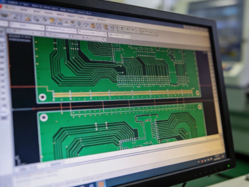
Before any order goes into production, our engineering team reviews the design files for manufacturability. This Dfm review catches potential issues before they cause problems in production, saving time and money for our customers. Typical Dfm checks include:
We provide detailed DFM reports to customers with specific recommendations for improving their designs, along with quotations that reflect the actual manufacturing requirements.
For new product introductions, we offer prototyping services that allow customers to validate their designs before committing to full production. Our prototyping team can produce small quantities of boards using the same processes and equipment as our production lines, ensuring that prototypes accurately represent production results.
We work closely with customers during the new product introduction (NPI) phase, fine-tuning assembly parameters, identifying and resolving issues, and preparing for volume production ramp-up.
Our engineering team also helps customers optimize their designs for cost, performance, and manufacturability. Value engineering reviews may identify opportunities to:
Modern Electronics Manufacturing must balance production efficiency with environmental responsibility. Our factory is committed to minimizing our environmental footprint through responsible practices at every stage.
Pcb Manufacturing is water-intensive, particularly in the plating and cleaning processes. Our facility operates closed-loop water recycling systems that treat and reuse process water, dramatically reducing freshwater consumption compared to older manufacturing methods. Wastewater treatment plants ensure that any discharge meets or exceeds local environmental regulations.
We strictly control the use and disposal of chemicals in our manufacturing processes. Hazardous materials are handled according to international standards including RoHS and REACH. Our chemical management system tracks all substances used in production, ensuring full traceability and regulatory compliance.
Where possible, we have transitioned to less hazardous alternatives. For example, we have implemented lead-free soldering processes throughout our facility, eliminating lead exposure risks for our employees and ensuring Rohs Compliance for our customers.
Our manufacturing processes generate various waste streams including metal scrap, plastic packaging, and chemical residues. We partner with licensed waste management companies for proper handling and disposal of all waste streams. Metal scrap from manufacturing is sold to recyclers, while waste electronics are processed through certified e-waste handlers.
We continuously work to reduce waste at the source through improved process controls, better material utilization, and packaging optimization programs.
Energy consumption represents a significant portion of our manufacturing costs and environmental impact. We have invested in energy-efficient equipment including Led Lighting, variable-frequency drives on motors, and advanced reflow ovens with improved thermal efficiency.
Solar panels on our factory roof generate a portion of our electricity needs, and we participate in renewable energy procurement programs to offset our remaining carbon footprint.
Behind every high-tech machine and automated process is a team of skilled, dedicated people. Our factory employs over 800 people across production, engineering, quality, logistics, and support functions. Many of our team members have been with us for over a decade, building deep expertise that translates into consistent quality for our customers.
Our production workforce is organized into dedicated teams for each major process area: drilling, plating, pattern transfer, solder mask, SMT assembly, through-hole assembly, testing, and inspection. Team leaders are responsible for daily production planning, quality monitoring, and continuous improvement activities within their areas.
We invest in cross-training to develop flexible teams that can respond to changing production demands. Our operators are encouraged to pursue skill certifications that recognize their growing expertise.
Our engineering department includes specialists in PCB design, process engineering, test engineering, and NPI management. Many of our engineers hold advanced degrees in electrical, mechanical, or chemical engineering. They are supported by CAD designers, process technicians, and documentation specialists.
We maintain active relationships with universities and technical schools, recruiting talent and providing internships that give students real-world manufacturing experience.
Quality is embedded throughout our organization, but our dedicated quality team provides the oversight, systems, and expertise that ensure consistent standards. Quality engineers work on process capability improvement, statistical analysis, and customer quality interface. Quality technicians perform inspections, manage test equipment, and maintain quality documentation.
Our sales and customer service teams serve as the primary interface with customers around the world. They are supported by technical account managers who understand both the customer's requirements and our manufacturing capabilities. This ensures clear communication and smooth order execution from inquiry through delivery.
To illustrate how our factory operates in practice, let us trace a typical order through its journey from receipt to shipment.
Morning: Customer service team reviews new orders received overnight. Engineering begins Dfm Review for any designs that require clarification. Production planning team reviews the production schedule and prepares materials staging for the day.
Mid-morning: First shift operators arrive and conduct shift handover briefings. Materials are staged at production line entry points. Quality technicians perform equipment calibration checks and verify that production conditions (temperature, humidity) are within specification.
Late morning: First boards of the day begin flowing through the production line. SPI systems monitor solder paste printing quality. Pick-and-place machines run at full speed. Reflow ovens reach stable operating temperature.
Midday: Shift changeover. AOI systems inspect the first completed boards. Any defects detected trigger immediate investigation and corrective action. Production continues through the lunch period with skeleton crews maintaining line flow.
Afternoon: ICT and functional testing begins on boards that have completed assembly. Test results are recorded and analyzed. Good boards move to final inspection and packaging, while defective boards are routed to rework or scrap areas.
Late afternoon: Completed boards are packaged according to customer specifications. Packaging includes anti-static trays or tubes, moisture barrier bags with desiccant, and proper labeling. Finished goods are staged for shipment.
Evening: Shipping documents are prepared and customs paperwork completed for international shipments. Trucks arrive to pick up outbound freight. End-of-day production reports are compiled and reviewed by production management.
A PCB factory is far more than a collection of machines and processes. It is a living ecosystem where people, technology, materials, and systems work together to create products that touch every aspect of modern life. From the smartphones in our pockets to the medical devices that save lives, the humble Printed Circuit Board is everywhere—and it takes extraordinary effort to make something ordinary look easy.
We hope this behind-the-scenes tour has given you a glimpse into the dedication, expertise, and investment required to manufacture world-class PCBs. Every board that leaves our facility represents thousands of decisions, hundreds of process steps, and the combined effort of hundreds of skilled professionals.
When you choose a PCB manufacturing partner, you are not just buying a board—you are investing in a relationship with a team that will stand behind every product they make. Quality, reliability, and continuous improvement are not marketing slogans; they are the operating principles that guide everything we do, every single day.
Thank you for taking this tour with us. We look forward to the opportunity to partner with you on your next electronics project.
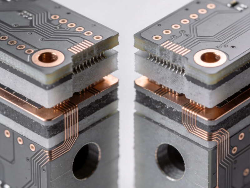
Microvias vs. Through-Holes: Choosing the Right Tech for Your Multilayer BoardAugust/06/2026
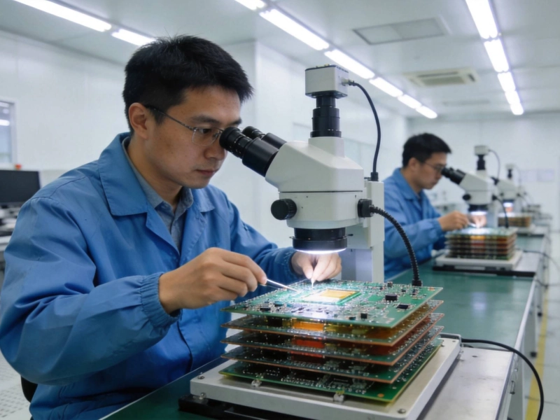
How We Ensure Quality Control in Multilayer PCB LaminationAugust/08/2026
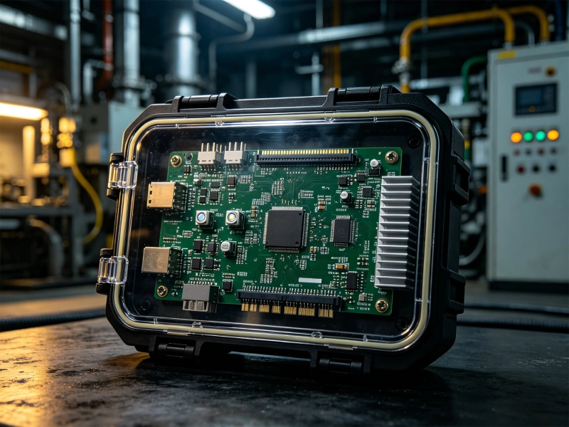
Durability Requirements for Industrial IoT PCBs: Ensuring Reliability in Harsh EnvironmentsSeptember/03/2026
How to Design High-Layer Count PCBs (20+ Layers) for Complex ElectronicsSeptember/08/2026
What Are Multilayer PCBs? A Complete Guide from ChinaMay/18/2026
Understanding HDI PCB Stack-ups: Best Practices for High-Density DesignsJuly/18/2026
What is HDI PCB? A Complete Guide from China HDI PCB ManufacturerMay/13/2026
Preparing Your Gerber Files for a Smooth China PCB Fabrication ProcessSeptember/18/2026