Open Nav
In the rapidly evolving world of electronics, miniaturization has become a driving force across virtually every industry. From smartphones that fit in your pocket to medical devices that can be implanted in the human body, the demand for smaller, lighter, and more powerful electronic products continues to grow. At the heart of this miniaturization revolution is HDI Pcb Technology—High Density Interconnect printed circuit boards that enable unprecedented levels of complexity and compactness in electronic packaging.
HDI PCBs have transformed how engineers design and manufacture electronic devices. By allowing more functionality in less space, HDI technology has become essential for everything from consumer electronics to aerospace applications. But what exactly makes HDI PCBs different from traditional boards, and why should you consider them for your next project?
This comprehensive guide covers everything you need to know about HDI Pcb Technology, from basic concepts to advanced manufacturing techniques, helping you make informed decisions about incorporating HDI into your designs.
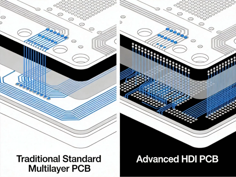
HDI (High Density Interconnect) PCB refers to a type of Printed Circuit Board that features a higher density of components and interconnections compared to traditional PCBs. This increased density is achieved through advanced design techniques, specialized materials, and sophisticated manufacturing processes.
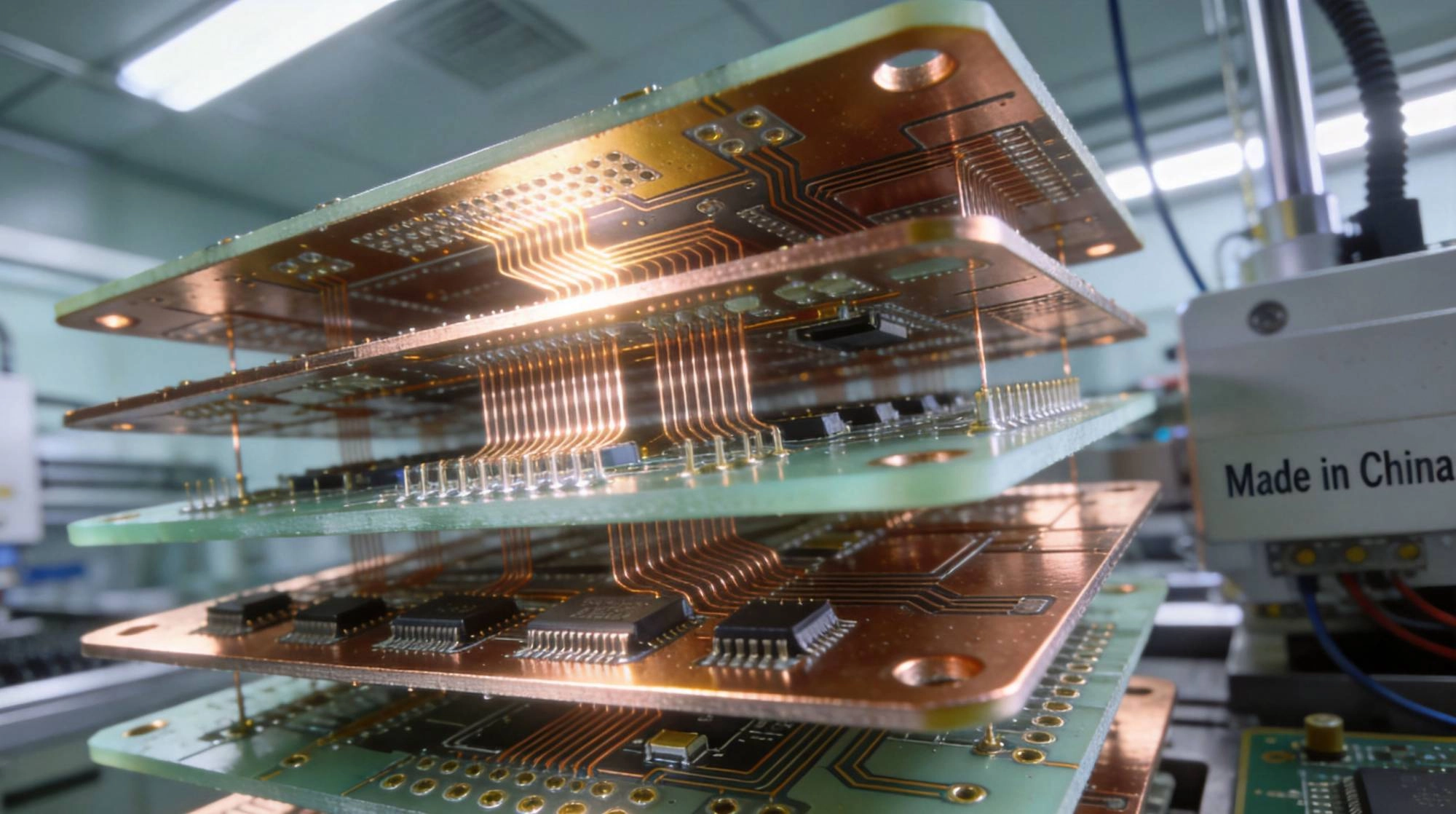
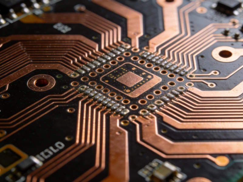
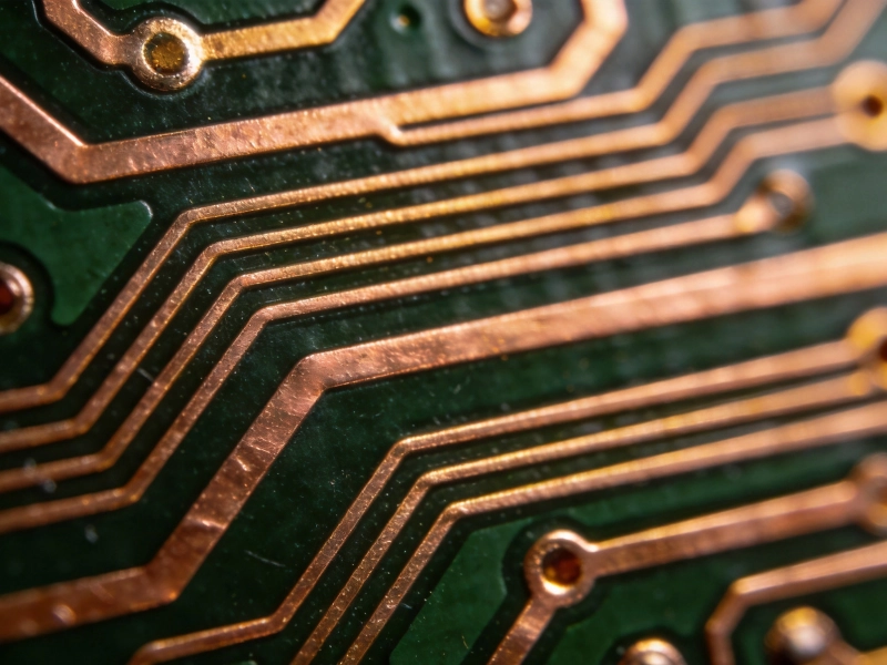
The key characteristic that defines HDI PCBs is the use of microvias—extremely small drilled holes that connect different layers of the board. These microvias, typically measuring less than 150 micrometers in diameter, allow for much tighter routing of signals between layers compared to traditional Through-hole Technology.
Understanding HDI construction requires familiarity with several key terms and concepts that define how these boards are built and function.
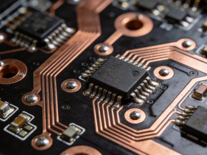
An Hdi Pcb consists of multiple layers of conductive copper traces separated by insulating dielectric material. Unlike traditional boards where all layers are connected through mechanical drilling of through-hole vias, HDI boards use a combination of via technologies:
HDI boards can be constructed using various build-up configurations, each offering different advantages:
1+N+1 Structure: This basic HDI configuration features one layer of microvia buildup on one or both sides of a core substrate. The "1" represents the buildup layers, "N" represents the number of core layers, and the second "1" represents optional additional buildup on the opposite side.
2+N+2 Structure: More complex than 1+N+1, this configuration allows for two layers of microvia buildup on each side of the core, enabling even higher density interconnections.
Any-Layer HDI: The most advanced configuration, any-layer HDI allows microvias to connect any two adjacent layers throughout the board. This maximum flexibility enables the highest density designs but requires the most sophisticated manufacturing capabilities.
HDI technology offers numerous advantages that make it the preferred choice for modern electronic applications:
The most obvious benefit of HDI PCBs is their ability to reduce board size while maintaining or increasing functionality. By using microvias and fine traces, designers can pack more components into smaller spaces. This is particularly valuable for:
Beyond space savings, HDI technology provides significant electrical advantages:
HDI technology enables more creative and efficient PCB layouts. Designers can place components on both sides of the board and route signals through any layer, opening up possibilities that would be impractical or impossible with traditional technology.
While HDI PCBs generally cost more per unit area than traditional boards, they can reduce overall system costs by:
HDI technology serves a wide range of industries and applications, from consumer gadgets to mission-critical systems.
The smartphone in your pocket represents one of the most demanding applications for HDI technology. Modern smartphones contain HDI PCBs with 10 or more layers, microvia counts in the thousands, and feature sizes measured in micrometers. Tablets, laptops, smartwatches, and wireless earbuds similarly rely on HDI technology to deliver powerful functionality in compact packages.
Medical electronics demand exceptional reliability and miniaturization. HDI PCBs enable:
Modern vehicles contain dozens of electronic control units, each requiring sophisticated PCB technology. HDI PCBs are used in:
In aerospace applications where reliability is paramount and weight savings translate directly to fuel efficiency, HDI PCBs provide essential capabilities:
Data centers and high-performance computing systems push the limits of PCB technology:
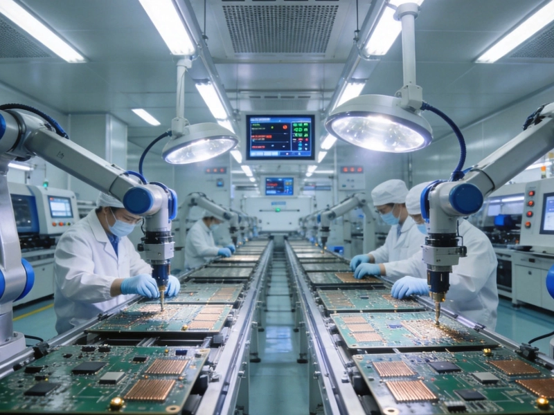
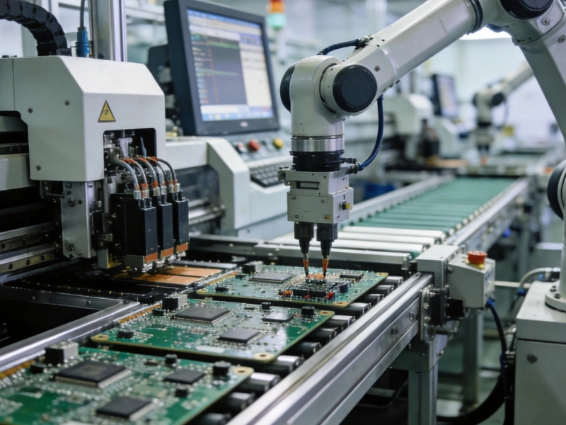
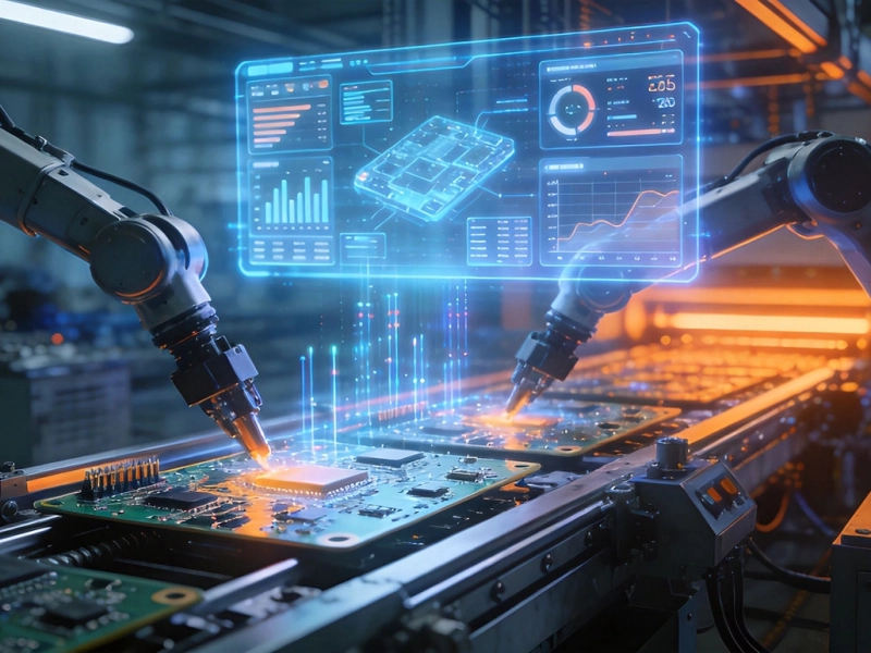
Manufacturing HDI PCBs requires specialized equipment, precise process control, and extensive expertise. Understanding the basic manufacturing flow helps appreciate the complexity involved.
Like traditional PCBs, HDI manufacturing begins with core substrate preparation. The core typically consists of fiberglass fabric pre-impregnated with epoxy resin (prepreg) laminated between Copper Foil layers. For advanced HDI applications, high-performance materials such as Rogers or Panasonic Megtron substrates may be used.
The defining characteristic of HDI manufacturing is the use of laser drilling to create microvias. CO2 and UV laser systems precisely ablate dielectric material to form vias as small as 50 micrometers. The laser drilling process:
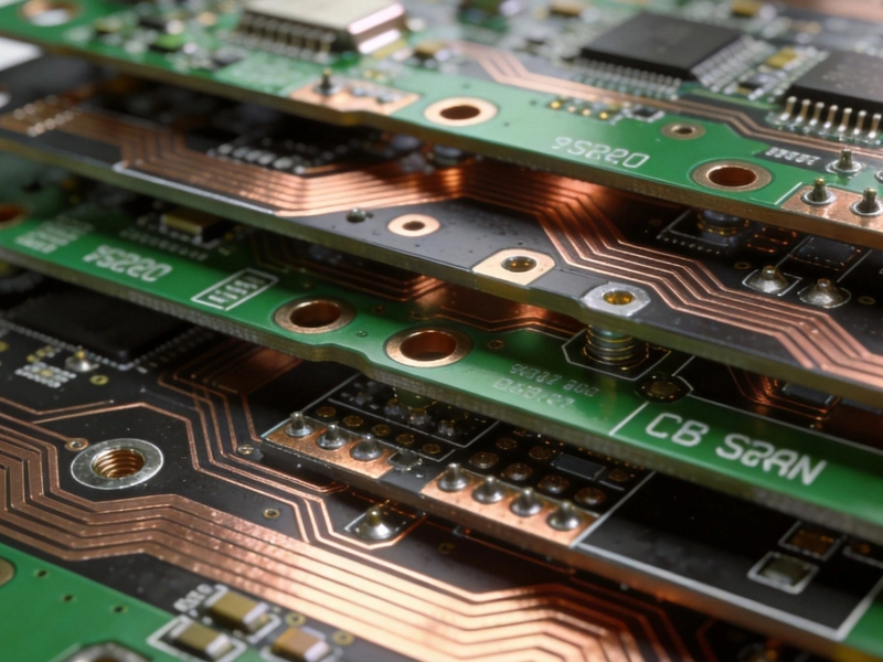
HDI boards are built up layer by layer through a process called Sequential Lamination. Each additional layer requires:
This process repeats until the desired layer count is achieved. Each step must be precisely controlled to ensure reliability and yield.
Creating reliable electrical connections in microvias requires sophisticated plating processes:
HDI boards require surface finishes that provide reliable soldering while maintaining planarity for fine-pitch components:
Successful HDI design requires careful attention to manufacturing capabilities and design-for-manufacturing (DFM) guidelines. Working closely with your Hdi Pcb manufacturer early in the design process significantly improves first-pass success.
HDI technology has defined capabilities that constrain design options:
The board stack-up must be designed with manufacturing constraints in mind:
High-density designs generate concentrated heat that must be managed effectively:
The most successful HDI projects involve early collaboration with manufacturers. This includes:
Selecting the right manufacturing partner is critical to HDI project success. Consider these factors when evaluating potential suppliers.
Assess the manufacturer's technical specifications against your requirements:
HDI manufacturing demands specialized expertise:
Robust quality processes prevent costly failures:
Excellent customer support improves project outcomes:
Understanding what drives HDI PCB costs helps in project planning and cost optimization.
Work with your manufacturer to optimize designs for cost:
HDI PCB technology continues to evolve, driven by the relentless push toward greater miniaturization and performance.
The HDI PCB market continues to expand as new applications emerge. Key growth areas include:
HDI PCB technology has fundamentally transformed electronic product design and manufacturing. By enabling unprecedented levels of miniaturization, improved electrical performance, and design flexibility, HDI boards make possible the advanced devices we rely on daily.
Whether you're designing the next generation of smartphones, developing medical devices that improve lives, or creating aerospace systems that push the boundaries of what's possible, understanding HDI technology is essential for success.
The key to successful HDI implementation lies in understanding both the capabilities and constraints of the technology, and in building strong partnerships with experienced manufacturers who can guide your project from concept to production. With proper planning, collaboration, and quality focus, HDI PCBs deliver the performance, reliability, and miniaturization that modern electronics demand.
Ready to explore HDI technology for your next project? Consult with an experienced HDI PCB manufacturer to discuss your specific requirements and discover how this advanced technology can help you achieve your design goals.
HDI PCBs differ from traditional PCBs primarily in their use of microvias (laser-drilled holes typically less than 150 micrometers in diameter), finer trace widths, and Sequential Lamination processes. These features enable significantly higher component density and improved electrical performance compared to traditional Through-hole Technology.
HDI PCBs typically cost 20-50% more than equivalent traditional boards, depending on complexity. However, they can reduce overall system costs by enabling smaller products, fewer boards, and simplified assembly. The cost premium is often justified by the performance benefits for miniaturized applications.
Standard HDI capabilities typically include microvias as small as 0.05-0.15mm diameter and line widths of 50-75 micrometers. Advanced HDI processes can achieve even finer features, though this requires specialized manufacturing capabilities and may affect cost and lead time.
HDI is essential for applications requiring miniaturization and high functionality: smartphones, tablets, wearable devices, medical implants, Automotive Electronics, aerospace systems, and high-performance computing hardware. Any product where size, weight, or performance constraints drive design decisions can benefit from HDI.
HDI PCB lead times typically range from 3-6 weeks for standard configurations, with more complex designs requiring 6-10 weeks or longer. Factors affecting lead time include layer count, feature complexity, material availability, and required testing. Planning ahead helps optimize delivery schedules.
HDI PCB Manufacturing Process: Step-by-Step ExplanationMay/13/2026
What is HDI PCB? A Complete Guide from China HDI PCB ManufacturerMay/13/2026
Top 5 Applications of HDI PCBs in Modern ElectronicsMay/13/2026
What is the Minimum Trace Width for HDI PCBs?July/17/2026
The Future of PCB Manufacturing in China: Trends for 2026 and BeyondMay/19/2026
Understanding HDI PCB Technology: A Comprehensive Guide for BeginnersMay/13/2026
Why Choose a China HDI PCB Manufacturer for Your Project?May/13/2026
HDI PCB vs Standard PCB: Key Differences ExplainedMay/13/2026