Open Nav
Modern electronics would be impossible without multilayer PCBs. Your smartphone contains a dozen or more multilayer boards, each packing incredible functionality into a fraction of a millimeter of thickness. Your laptop, your car, your medical devices—all rely on multilayer technology to achieve the density and performance that consumers expect.
But what exactly is a multilayer PCB? How do the layers work together? When should you choose multilayer over simpler alternatives? And what do you need to know as an engineer to design them effectively? This guide answers these questions with the depth working engineers need to make informed decisions about multilayer technology.
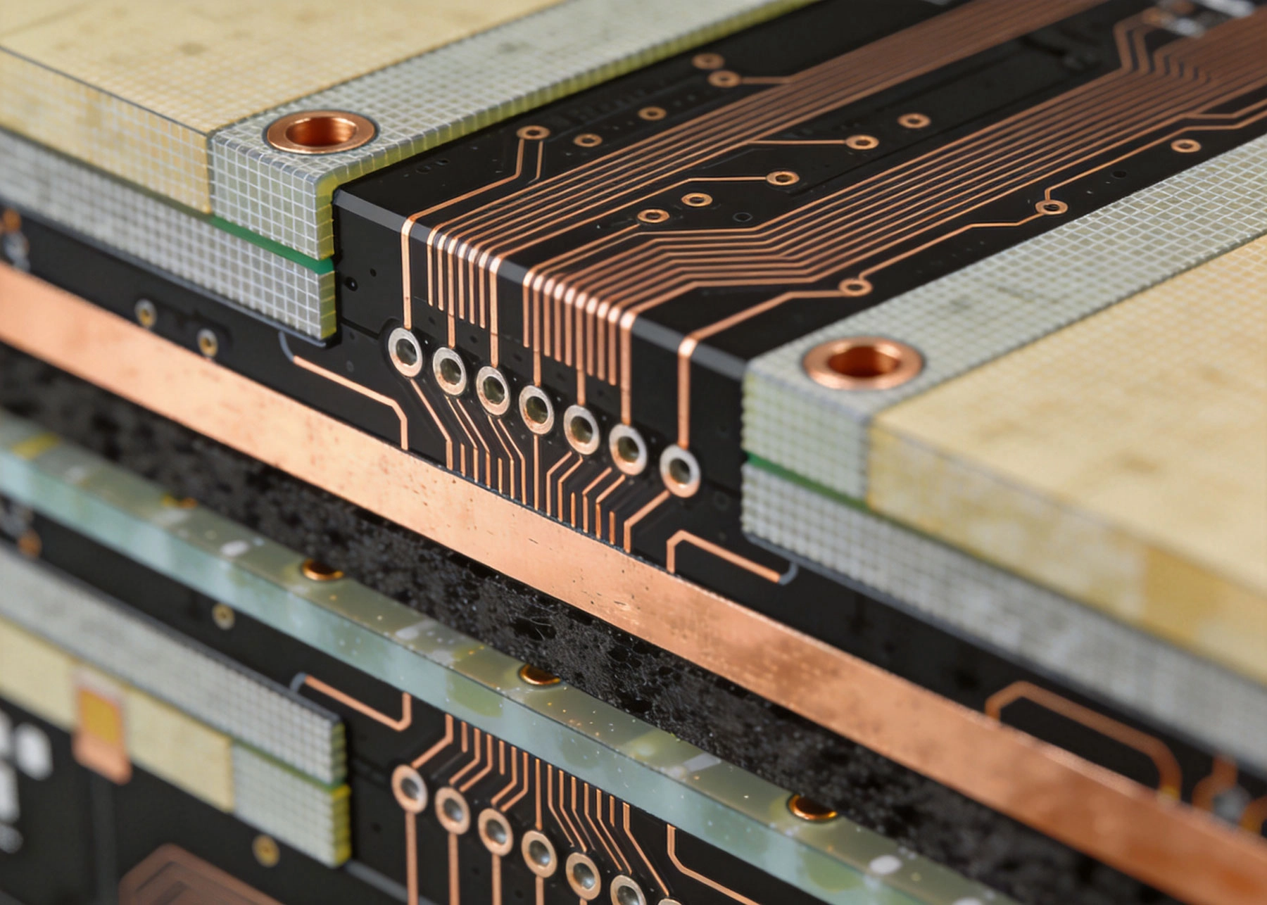
A multilayer PCB is simply a Printed Circuit Board with more than two conductive layers. While a simple double-sided board has copper on the top and bottom surfaces only, multilayer boards sandwich additional copper layers between insulating dielectric materials, creating a three-dimensional interconnect structure.
The layers are laminated together under heat and pressure, forming a unified board that functions as a single component. Electrical connections between layers are made through plated holes called vias, which can extend through all layers (through-hole vias), connect only specific layers (blind or buried vias), or link adjacent layers only (microvias).
Multilayer boards range from 4 layers (the minimum to technically qualify as multilayer) to 50+ layers for extreme applications like supercomputers and aerospace systems. Most consumer electronics use 4-12 layers, with smartphones typically at 8-12 layers and laptops at 10-16 layers.
The fundamental reason for multilayer construction is routing density. As electronic components shrink and pin counts increase, there simply isn't enough surface area on two layers to route all the necessary connections. Internal layers provide additional routing space while maintaining the board's physical size.
But routing density isn't the only advantage. Multilayer construction also enables:
The layer stackup—the specific arrangement of signal, power, and ground layers—is the foundational decision in multilayer Pcb Design. Get the stackup wrong, and no amount of clever routing will produce a working board.
The simplest multilayer configuration is the 4-layer board, which typically follows this structure:
This arrangement places signal layers adjacent to reference planes (ground on layer 2, power on layer 3), which provides controlled impedance for high-speed signals and reduces electromagnetic interference. The ground and power planes also distribute power more effectively than traces, reducing voltage drop and noise.
As layer count increases, stackup options multiply. A typical 6-layer stackup might be:
This arrangement maintains signal layers adjacent to reference planes while adding routing layers in the center. The exact arrangement depends on your specific requirements—some designs might dedicate more layers to power distribution, others to signal routing, others to shielding.
Higher layer counts follow similar principles but with more flexibility. An 8-layer board might have two ground planes, two power planes, and four signal layers arranged to minimize crosstalk and provide adequate return paths for all signals.
Multilayer boards are built from cores and prepreg materials. Cores are fully cured fiberglass-epoxy laminates with Copper Foil bonded to both sides. Prepreg (pre-impregnated) is partially cured fiberglass cloth that flows and bonds layers together during lamination.
The stackup alternates cores and prepreg layers. For example, a 4-layer board might use a thick core for the center, with thin prepreg and foil on the outer layers. Or it might use two thin cores with prepreg between them—different approaches that affect final thickness, electrical properties, and manufacturing characteristics.
The dielectric constant (Dk) and thickness of cores and prepreg affect signal propagation, impedance, and capacitance. These parameters must be specified carefully and coordinated with your PCB manufacturer to ensure they can achieve the values your design requires.
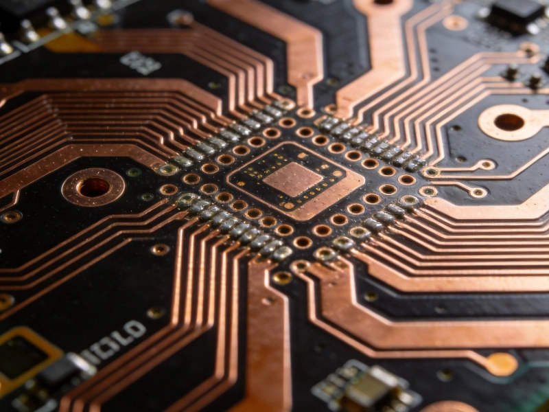
Vias are the vertical interconnects that make multilayer boards function. Understanding the different via types and their characteristics is essential for effective multilayer design.
Through-hole vias extend through the entire board thickness, connecting all layers. They're mechanically drilled and then plated with copper to create electrical connections. Through-hole vias are the most robust and reliable via type but consume space on all layers and create stubs on layers where the connection isn't needed.
For high-speed designs, through-hole vias create impedance discontinuities and signal reflections. The portion of the via that extends beyond the connected layers (the stub) acts as an unterminated transmission line, causing signal integrity problems at high frequencies.
Blind vias connect an outer layer to one or more inner layers without penetrating through the entire board. They can be created by drilling before final lamination or by laser drilling after partial lamination. Blind vias save space on layers that don't need the connection and eliminate stub effects on those layers.
Blind vias add manufacturing complexity and cost. They require Sequential Lamination processes and careful alignment. But for high-density designs where routing space is at a premium, blind vias are often essential.
Buried vias connect internal layers only, with no connection to outer layers. They're completely hidden within the board structure. Like blind vias, they require Sequential Lamination and add cost, but they provide routing flexibility without consuming outer layer space.
Buried vias are particularly useful in HDI (High Density Interconnect) designs where outer layers are crowded with fine-pitch components and need maximum routing space.
Microvias are small vias (typically 0.15mm diameter or less) that connect only adjacent layers. They're created by laser drilling and are a key technology in HDI boards. Microvias enable extremely high routing density and are essential for modern smartphone and tablet designs.
Microvias can be stacked (multiple microvias aligned vertically to connect non-adjacent layers) or staggered (offset to reduce manufacturing difficulty). Stacked microvias provide the shortest path between layers but are more challenging to manufacture reliably.
Multilayer design requires attention to several factors that don't apply to simpler boards. Understanding these considerations helps you create designs that are manufacturable, reliable, and cost-effective.
High-speed signals require careful attention to return paths, impedance control, and crosstalk. In multilayer boards, these concerns are managed through layer stackup and routing discipline.
Every high-speed signal needs a continuous return path in an adjacent reference plane (ground or power). If the return path is interrupted—by a split in the plane, a via transition without a nearby ground via, or a long trace without plane reference—impedance discontinuities and EMI result.
Impedance control requires specifying trace widths based on the dielectric thickness to the reference plane and the dielectric constant of the material. These calculations must account for the actual stackup that will be manufactured, not just theoretical values.
Crosstalk between signals is minimized by maintaining adequate spacing, routing adjacent layers orthogonally (one layer horizontal, next layer vertical), and using ground planes between aggressive signal layers.
Multilayer boards typically dedicate entire layers to power distribution rather than using traces. Solid power planes provide lower impedance power distribution, reduce voltage drop under load, and improve decoupling effectiveness.
Multiple power planes may be needed for different voltage rails. These planes can be arranged on a single layer (split planes) or on separate layers. Split planes create discontinuities that affect return paths for signals crossing the split, so their placement requires careful consideration.
Decoupling capacitors connect power and ground planes, providing local charge storage and filtering high-frequency noise. Their placement and connection to planes affect power integrity significantly.
Heat-generating components require thermal management that leverages multilayer construction. Thermal vias—arrays of vias connecting surface pads to internal copper planes—provide heat conduction paths from components to the board interior where heat can spread.
Copper weight (thickness) affects thermal conductivity. Thicker copper on internal layers improves heat spreading but increases cost and affects fine-feature manufacturability. Some designs use thick copper on specific layers dedicated to thermal management while keeping signal layers at standard copper weight.
Not everything that can be drawn can be manufactured reliably. Multilayer boards have specific constraints that designers must respect:
These constraints vary by manufacturer and should be confirmed before finalizing a design. What one shop can manufacture reliably, another might struggle with.
Understanding how multilayer boards are manufactured helps you design boards that can be built reliably and economically.
Multilayer manufacturing starts with inner layers. Each core layer is processed individually—cleaned, coated with photoresist, exposed with the layer artwork, developed, and etched to create the copper pattern. Automated optical inspection (AOI) checks each inner layer for defects before lamination.
The processed cores and prepreg layers are stacked in the specified order and placed in a lamination press. Heat and pressure cause the prepreg to flow and bond the layers together, while also curing the resin to create a solid, unified board. Temperature, pressure, and time profiles are carefully controlled to ensure proper bonding without defects.
After lamination, holes are drilled for vias and component mounting. Multilayer drilling requires high precision to maintain alignment between layers. The drilled holes are then plated with copper to create electrical connections between layers.
For boards with blind and buried vias, multiple drilling and plating operations occur at different stages of the Manufacturing Process, which is why these via types add cost and complexity.
Outer layers receive the same photoresist coating, exposure, and etching as inner layers. The plating process also deposits additional copper on outer layer traces to achieve the specified copper weight. Finally, solder mask is applied to protect the board, and surface finish (ENIG, HASL, etc.) is applied to exposed copper.
Electrical testing verifies that all connections are correct and there are no shorts or opens. For multilayer boards, this is essential—internal layer defects aren't visible and can only be detected through electrical testing. Additional inspection steps include AOI of outer layers and cross-section analysis of sample boards to verify internal structure.
Multilayer boards aren't always necessary or appropriate. Understanding when they provide value helps you make the right technology choice.
The cost difference between double-sided and 4-layer boards has narrowed significantly—often only 20-30% more for 4-layer. For this reason, many designers default to 4-layer even when double-sided might suffice, trading slightly higher cost for improved signal integrity and easier routing.
Multilayer boards cost more than simpler alternatives, but the cost drivers aren't always obvious. Understanding these factors helps you optimize for cost without compromising functionality.
Each additional layer increases cost—more material, more processing steps, more opportunities for defects. The relationship isn't strictly linear, but going from 4 to 6 layers typically increases cost 30-50%, and going from 6 to 8 adds another similar increment. Very high layer counts (20+) enter premium territory where costs increase rapidly.
Larger boards use more material and processing time. But complexity—feature density, via count, trace width—often matters more than raw size. A small, dense board with fine traces and many vias can cost more than a larger, simpler board.
Features that add manufacturing complexity increase cost:
Every special feature should be justified by functional requirements. Don't specify blind vias "just in case" if through-hole vias will work.
Multilayer technology appears across virtually every electronics sector. Understanding typical applications helps you recognize when multilayer is the standard approach in your industry.
Smartphones, tablets, laptops, and wearables are all multilayer applications. Smartphones typically use 8-12 layer HDI boards with microvias. Laptops use 10-16 layers to accommodate processors, memory, and high-speed interfaces. Even simple consumer devices often use 4-layer boards for improved EMC and easier routing.
Routers, switches, and base stations use multilayer boards to handle high-speed signals and complex processing. High-frequency RF sections might use specialized materials, but the digital processing sections are typically standard multilayer FR-4.
Modern vehicles contain dozens of ECUs (electronic control units), each typically on 4-6 layer boards. Infotainment systems, ADAS (advanced driver assistance), and electric powertrain controls use higher layer counts and more advanced technologies.
Medical electronics range from simple 2-layer devices to complex 16+ layer imaging and diagnostic equipment. Reliability requirements often drive conservative designs with proven materials and manufacturing processes.
Industrial controls, military systems, and aerospace applications use multilayer boards extensively. These applications often emphasize reliability and environmental tolerance over density, leading to conservative designs with adequate margins.
Multilayer PCBs are essential technology for modern electronics, enabling the density, performance, and reliability that products require:
For working engineers, multilayer Pcb Technology is no longer exotic—it's the standard approach for anything beyond the simplest designs. Understanding how to design and specify multilayer boards effectively is a core competency for Electronics Development.
Technically, a multilayer PCB has more than two layers, so 4 layers is the minimum. In practice, 4-layer boards are the simplest multilayer configuration and are extremely common. They're often only modestly more expensive than double-sided boards while providing significant routing and signal integrity benefits.
Standard multilayer boards are typically 1.6mm thick, the same as double-sided boards. However, thickness varies with layer count and design requirements. High-layer-count boards might be thicker (2.0-3.2mm) to accommodate all layers, while thin multilayer boards for mobile devices might be 0.8mm or less. The specific thickness depends on the stackup design and material thicknesses.
Yes, though multilayer prototypes cost more than double-sided. Quick-turn prototype shops offer 4-layer boards at reasonable prices, and even 6-8 layer prototypes are accessible for most projects. The key is ordering small quantities (5-10 pieces) for initial validation before committing to larger production runs. The cost difference between 2-layer and 4-layer prototypes has narrowed considerably, making 4-layer the default for many designers.
Start by estimating your routing requirements—component count, pin density, and signal types. Simple designs with few high-speed signals might work on 4 layers. Complex digital designs with DDR memory interfaces typically need 6-8 layers. Very dense designs with fine-pitch components might require 10+ layers or Hdi Technology. When in doubt, consult with your PCB manufacturer—they can review your design and recommend appropriate layer counts based on their capabilities and your requirements.
Properly designed and manufactured multilayer boards are highly reliable. The lamination process creates a solid, unified structure that withstands thermal cycling, vibration, and environmental stress. Reliability issues typically stem from design errors (inadequate clearances, improper via design) or manufacturing defects (delamination, plating problems), not from the multilayer concept itself. Following design guidelines and working with qualified manufacturers produces reliable multilayer boards.

Understanding PCB Assembly Prices in China: What Factors Influence Cost?June/10/2026

The Complete Step-by-Step Process ExplainedJune/05/2026
PCB Assembly Price China: A Complete Cost Guide for 2024May/18/2026

Detailed Explanation of the Types, Materials, and Applications of Flexible Circuit Boards 101June/04/2026
The Role of Heavy Copper PCBs in Electric Vehicle Battery Management SystemsJune/26/2026
What is HDI PCB? A Complete Guide from China HDI PCB ManufacturerMay/13/2026
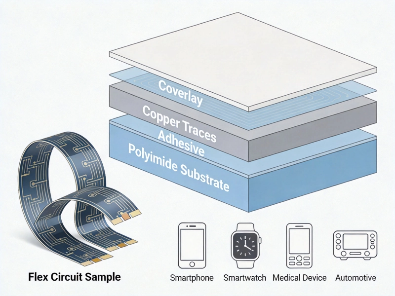
Introduction to Flexible Printed Circuit Boards (FPC): Beginner's GuideMay/18/2026
The Ultimate Guide to HDI PCB Technology You Need to KnowJune/02/2026