Open Nav
The electronics industry is undergoing a remarkable transformation. As devices become smaller, more complex, and increasingly portable, traditional Printed Circuit Board designs are facing significant limitations. Rigid-flex Pcb design has emerged as a revolutionary solution, combining the structural integrity of rigid boards with the flexibility needed for modern applications. This comprehensive guide explores everything you need to know about Rigid-flex Pcb design, from fundamental concepts to advanced implementation strategies.
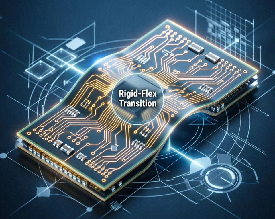
Rigid-Flex Pcb Design represents a hybrid approach to circuit board manufacturing. It integrates both rigid and flexible circuit materials into a single unified assembly. The rigid sections provide structural support and accommodate heavy components, while flexible sections enable the board to bend, fold, or conform to complex three-dimensional shapes. This innovative design approach has gained tremendous traction, with the market experiencing an 18% annual growth rate driven by wearable devices and foldable terminals.
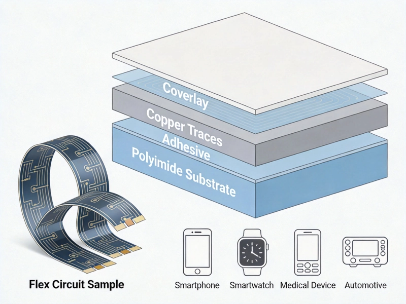
The fundamental principle behind Rigid-Flex Pcb Design lies in its multi-layered construction. Typically, flexible polyimide or polyester materials form the bendable regions, while FR-4 materials create the rigid sections. These components are laminated together using advanced bonding techniques, creating a seamless transition between rigid and flexible zones. The result is a versatile circuit board that can replace multiple separate boards and interconnects, reducing assembly complexity and improving reliability.
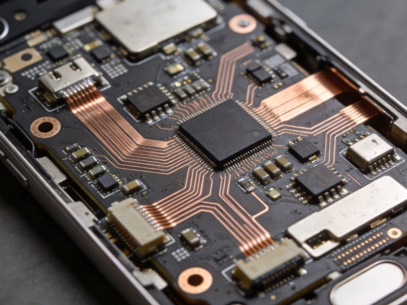
Adopting Rigid-Flex PCB design offers numerous advantages that make it increasingly attractive across diverse industries. One of the most significant benefits is space efficiency. By eliminating bulky connectors and reducing the number of separate boards, designers can create more compact products without sacrificing functionality. This space optimization has proven crucial in applications like smartphones, medical implants, and aerospace systems where every millimeter matters.
Enhanced reliability stands as another compelling advantage. Traditional rigid boards with flexible cables at their connections are prone to failure at the junction points. Rigid-Flex PCB design eliminates these weak spots by creating continuous electrical pathways. The seamless transition between rigid and flexible sections significantly reduces stress concentrations, resulting in longer product lifespans and reduced maintenance requirements. Industry studies have shown that Rigid-Flex designs can reduce connection failures by up to 90% compared to traditional approaches.
Cost reduction, though perhaps counterintuitive given the higher material costs, represents another key benefit. While individual Rigid-Flex boards may cost more than their rigid counterparts, the overall system cost often decreases. Fewer components mean less assembly time, reduced inventory management complexity, and lower total bill of materials. For complex systems requiring multiple interconnected boards, the total cost savings can reach 30-40% when implementing Rigid-Flex PCB design strategies.
The design flexibility offered by Rigid-Flex technology enables innovative product architectures that would be impossible with traditional rigid boards. Designers can create three-dimensional circuit layouts that conform to product shapes, optimize signal paths, and reduce electromagnetic interference. This freedom has led to breakthrough designs in consumer electronics, military applications, and medical devices where space constraints and reliability requirements are paramount.
Successful Rigid-Flex PCB design requires careful attention to several critical factors. Material selection serves as the foundation of any robust design. Designers must choose appropriate materials for both rigid and flexible sections, considering factors like thermal expansion coefficients, dielectric properties, and mechanical strength. Polyimide materials, such as Kapton, are commonly used for flexible areas due to their excellent thermal stability and mechanical durability, while FR-4 remains the standard for rigid sections.
The transition zones between rigid and flexible areas demand special consideration. These regions experience the highest mechanical stress during bending and must be carefully designed to prevent failure. Engineers typically employ "tear-drop" or arc-shaped routing patterns to distribute stress evenly. The placement and spacing of vias in these transition zones also require meticulous planning to maintain structural integrity while ensuring proper electrical connectivity.
Bend radius specifications play a crucial role in Rigid-Flex PCB design. Each flexible material has a minimum bend radius that must not be exceeded to prevent damage to copper traces and dielectric layers. Designers must consider both static bending (one-time bending during assembly) and dynamic bending (repeated bending during operation) scenarios. Dynamic applications typically require larger bend radii and more robust design approaches to ensure longevity under repeated flexing cycles.
Layer stack-up design represents another critical consideration. Rigid-Flex boards often feature asymmetric stack-ups where different numbers of layers exist in rigid versus flexible sections. Designers must carefully manage impedance control, signal integrity, and power distribution across these varying stack-ups while ensuring proper alignment and registration between layers. Advanced PCB design software with dedicated Rigid-Flex capabilities is essential for managing these complex requirements.
The Rigid-Flex PCB design process begins with a thorough requirements analysis. Designers must define electrical specifications, mechanical constraints, environmental conditions, and cost targets. This phase involves evaluating whether Rigid-Flex technology offers advantages over traditional approaches for the specific application. Key questions include space constraints, number of required interconnections, expected bending frequency, and temperature operating ranges. A detailed feasibility study at this stage prevents costly redesigns later in the process.
Once requirements are established, mechanical design takes center stage. Creating accurate 3D models of the board layout, including all bend areas and component placements, helps identify potential issues early. This step involves determining bend locations, bend radii, and stack-up configurations. Designers must account for how the board will flex in actual use, ensuring that components don't interfere with bending areas and that stress distributions remain within acceptable limits. Modern CAD tools with integrated Rigid-Flex capabilities enable real-time visualization of how boards will flex during operation.
With mechanical constraints understood, electrical design proceeds. This phase involves creating schematics that account for the unique requirements of Rigid-Flex PCB design. Designers must plan signal routing across rigid-flex transitions, manage impedance requirements, and ensure proper grounding strategies. Special attention must be paid to power distribution networks, as varying layer counts across rigid and flexible sections can create challenges for power plane continuity. Simulation tools help verify signal integrity and power delivery performance before moving to layout.
The layout phase is where Rigid-Flex PCB design becomes most intricate. Designers must route traces while respecting bend radius requirements, managing stress concentrations, and maintaining signal quality. Routing in flexible areas typically requires wider traces with rounded corners rather than sharp 90-degree angles. The placement of components near bend areas requires careful consideration to avoid stress concentrations that could cause component failure. Advanced routing algorithms specifically designed for Rigid-Flex boards help optimize trace placement while meeting all mechanical and electrical requirements.
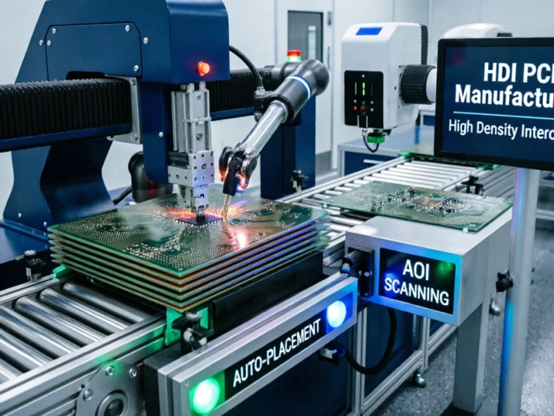
Comprehensive verification ensures the design meets all requirements before manufacturing. This phase includes design rule checks (DRC), electrical rule checks (ERC), and specialized Rigid-Flex verification routines. Designers verify bend area integrity, stress distributions, impedance matching, and thermal performance. Prototype fabrication and testing often follow simulation verification, providing real-world validation of design assumptions. This iterative process helps identify and resolve issues before full-scale production begins.
One of the most persistent challenges in Rigid-Flex PCB design is managing mechanical stress in bend areas. Repeated bending cycles can cause trace cracking, delamination, and eventual failure. The solution involves a multi-faceted approach: using appropriate materials with good fatigue resistance, optimizing trace routing with gentle curves and adequate widths, and implementing stress relief features. Strategic placement of stiffeners and proper lamination techniques also help distribute stress evenly and extend board lifetime.
Managing characteristic impedance across varying stack-up configurations presents significant difficulties. Different dielectric materials, layer counts, and thicknesses in rigid versus flexible sections can cause impedance discontinuities that affect signal integrity. Addressing this challenge requires careful impedance modeling and simulation, using controlled dielectric materials with consistent properties, and implementing impedance matching techniques at transitions. Some designers employ differential signaling with tightly coupled pairs to improve immunity to impedance variations.
Thermal management becomes particularly complex in Rigid-Flex PCB design due to varying thermal expansion coefficients between materials. Differential expansion can cause delamination, stress concentrations, and reliability issues. Solutions include selecting materials with compatible thermal expansion characteristics, implementing proper venting in bend areas to prevent heat buildup, and using thermal relief structures where appropriate. Some designs incorporate specialized thermal interface materials to improve heat dissipation across rigid-flex transitions.
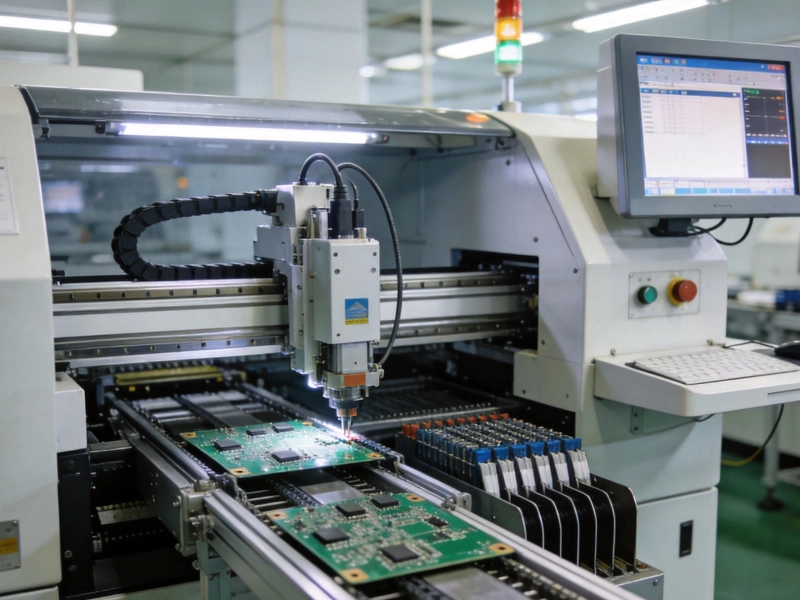
The Manufacturing Process for Rigid-Flex boards involves more steps and tighter tolerances than traditional rigid boards. Lamination, drilling, plating, and etching processes must account for both rigid and flexible materials simultaneously. Working closely with experienced manufacturers who have established Rigid-Flex capabilities is essential. Design-for-manufacturing (DFM) guidelines specific to Rigid-Flex technology help optimize designs for manufacturability while maintaining performance requirements. Clear communication between design and manufacturing teams prevents misunderstandings that could lead to costly iterations.
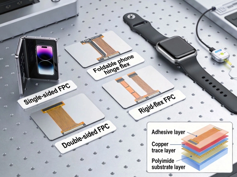
Rigid-Flex PCB design has found widespread adoption across diverse industries, each leveraging its unique advantages for specific applications. In consumer electronics, smartphones and tablets extensively use Rigid-Flex technology to maximize space utilization and improve durability. The ability to fold and bend circuitry enables innovative form factors while maintaining high reliability under daily use. Wearable devices represent another growing application area, where flexibility and comfort are essential requirements.
The medical device industry has embraced Rigid-Flex PCB design for implantable devices, diagnostic equipment, and portable medical instruments. The reliability improvements and space savings translate directly into better patient outcomes and more effective medical solutions. Military and aerospace applications leverage Rigid-Flex technology for avionics, satellites, and communication equipment where weight reduction and reliability are mission-critical factors. The automotive industry increasingly uses Rigid-Flex designs in infotainment systems, sensor arrays, and emerging autonomous vehicle technologies.
Industrial automation and robotics benefit from Rigid-Flex PCB design's ability to withstand harsh environments while providing reliable connectivity. Robotic joints and moving mechanisms can incorporate flexible circuitry that eliminates the need for slip rings or other traditional interconnection methods. As the Internet of Things (IoT) expands, Rigid-Flex technology enables more compact, reliable sensor nodes and edge computing devices that can conform to various form factors and installation environments.
Rigid-Flex PCB design has emerged as a transformative technology that bridges the gap between traditional rigid boards and flexible circuits. By combining the structural integrity of rigid materials with the adaptability of flexible circuits, designers can create innovative electronic products that were previously impossible. The benefits—space efficiency, improved reliability, cost reduction, and design flexibility—make Rigid-Flex technology increasingly attractive across industries.
Success in Rigid-Flex PCB design requires careful attention to material selection, mechanical design, electrical performance, and manufacturing considerations. By following established design processes and addressing common challenges proactively, designers can leverage this technology to create robust, reliable, and innovative electronic products. As material science advances and design tools continue to improve, we can expect even greater adoption of Rigid-Flex PCB design in the coming years.
The future of Rigid-Flex technology looks promising, with ongoing developments in materials science, manufacturing processes, and design methodologies. Emerging applications in flexible displays, Wearable Technology, and implantable medical devices will continue to drive innovation in this field. By mastering Rigid-Flex PCB design principles today, engineers position themselves to meet tomorrow's electronic design challenges and create products that define the cutting edge of technology.
Ready to implement Rigid-Flex PCB design in your next project? Partner with experienced manufacturers who specialize in this technology, and invest in advanced design tools that support Rigid-Flex workflows. The investment in proper design, analysis, and testing will pay dividends in product reliability, performance, and market success. Rigid-Flex PCB design isn't just about bridging the gap between rigid and flexible—it's about bridging the gap between today's possibilities and tomorrow's innovations.
Rigid-Flex PCB design integrates both rigid and flexible sections into a single unified assembly, whereas traditional flexible circuits are entirely bendable. The rigid sections provide structural support for heavy components and connectors, while flexible sections enable bending and folding. This hybrid approach combines the benefits of both technologies in a single board, reducing interconnections and improving reliability.
While individual Rigid-Flex boards typically cost 30-50% more than comparable rigid boards, the total system cost often decreases. When considering the complete system—including connectors, assembly time, inventory management, and reliability improvements—Rigid-Flex designs can actually reduce total costs by 30-40% for complex systems requiring multiple interconnected boards. The break-even point depends on the specific application and complexity.
The minimum bend radius depends on the specific materials used, number of layers, and application requirements. As a general guideline, static bending (one-time bend during assembly) typically allows bend radii of 3-6 times the total laminate thickness, while dynamic bending (repeated flexing) requires larger radii of 10-20 times the thickness. Always consult material specifications and design guidelines from your manufacturer for precise bend radius requirements.
Repairing Rigid-Flex PCBs is significantly more challenging than traditional rigid boards due to their complex layered construction. While some repairs in rigid sections may be possible, damage to flexible areas or transition zones typically requires board replacement. This is why proper design, thorough testing, and quality manufacturing are particularly important for Rigid-Flex assemblies. Preventing damage through careful design and proper handling is far more effective than attempting repairs.
Specialized PCB design software with dedicated Rigid-Flex capabilities is essential for successful implementation. Leading tools like Altium Designer, Cadence Allegro, Mentor Graphics Xpedition, and Siemens PADS Professional offer specific features for Rigid-Flex design, including 3D modeling, bend area visualization, stack-up management, and DFM checking. These tools help manage the unique challenges of Rigid-Flex design and improve first-pass success rates. Investing in appropriate design tools is crucial for efficient Rigid-Flex PCB development.
Introduction to Flexible Printed Circuit Boards (FPC): Beginner's GuideMay/18/2026
What is Flexible PCB? Complete Guide from China Flex PCB ManufacturerMay/18/2026
Introduction to Flexible Printed Circuit Boards: A Practical Engineering GuideMay/18/2026
SMT PCB Assembly China: A Complete Guide for Global BuyersMay/18/2026
How to Choose the Best China HDI PCB Manufacturer in 2026June/08/2026
Why Choose a China HDI PCB Manufacturer for Your Project?May/13/2026
High-Voltage Industrial Control Boards: The Case for Heavy CopperJune/29/2026
HDI PCB vs Standard PCB: Key Differences ExplainedMay/13/2026