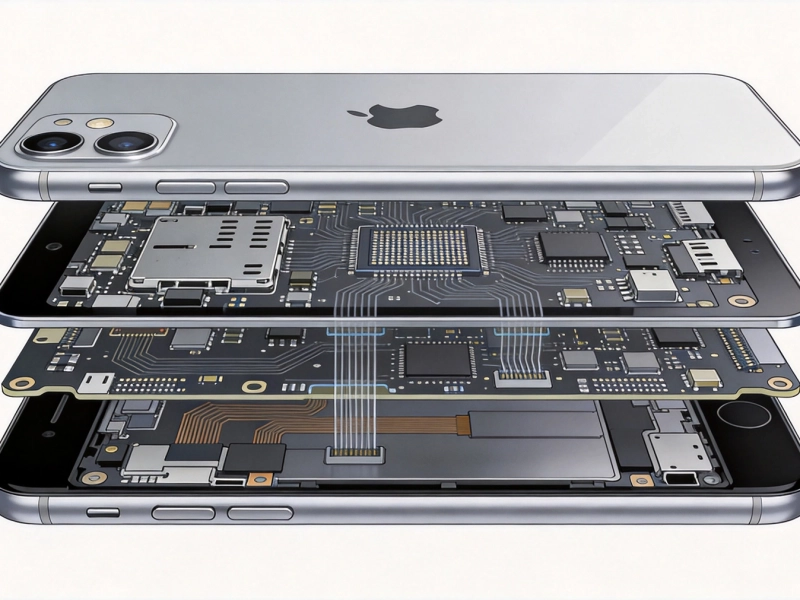
When you pickup your smartphone, power on your laptop, or start your car, you are interacting with products that rely on printed circuit boards—PCBs. These thin boards dotted with copper pathways are the backbone of modern electronics. But have you ever wondered how these intricate boards are actually made? The answer often leads to China's vast manufacturing ecosystem, where advanced facilities produce millions of PCBs every year for companies worldwide.
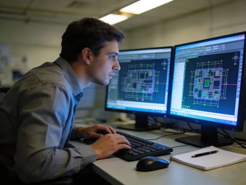
Understanding the Pcb Fabrication process helps engineers, product designers, and procurement specialists make better decisions. Whether you're sourcing prototypes or planning mass production, knowing what happens inside a Chinese Pcb Factory can give you a competitive edge. This guide walks you through each stage of Pcb Manufacturing, from raw materials to the final quality checks.
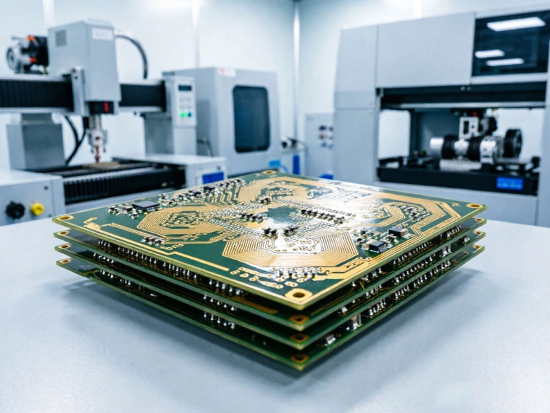
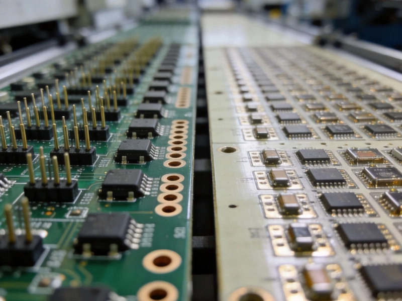
Pcb Fabrication is the process of manufacturing blank circuit boards—boards without any components soldered onto them. This is different from Pcb Assembly (PCBA), where electronic parts are added to the board. The fabrication stage transforms basic materials like copper-clad laminate into functional boards ready for component mounting.
China dominates global Pcb Production, accounting for over half of the world's output. Chinese manufacturers offer advantages in scale, cost efficiency, and increasingly, technical capability. From simple single-layer boards to complex multilayer designs with 20+ layers, Chinese factories handle it all.
The process starts with copper-clad laminate (CCL), the foundation material for most PCBs. This substrate typically consists of glass fiber fabric impregnated with epoxy resin, with thin Copper Foil bonded to one or both sides. Common grades include FR-4 (the most widely used), and high-performance materials like Rogers or polyimide for specialized applications.
Factory workers cut the large CCL sheets into smaller panels that match production requirements. Precision cutting ensures consistent dimensions, which prevents alignment issues in subsequent steps. Most Chinese factories use CNC-controlled cutting machines for accuracy. The standard panel sizes are 18×24 inches, 21×25 inches, or custom dimensions based on customer needs.
After cutting, the panels go through cleaning to remove any contamination, oils, or oxidation from the copper surface. This preparation step is crucial—any residue can cause defects in the finished board.
For multilayer PCBs, the Manufacturing Process begins with creating the inner layers. This stage transfers the circuit pattern onto the copper surface using a photolithographic method.
First, the panel receives a layer of photosensitive dry film resist. A film artwork containing the circuit design is then placed over the panel and exposed to ultraviolet light. The UV exposure hardens the resist in areas where the circuit should remain, while unexposed areas stay soft. After exposure, a chemical developer removes the soft resist, leaving behind a protective pattern that matches the desired circuitry.
Next comes etching—the crucial step where unwanted copper gets dissolved. The panel is sprayed with alkaline solutions that eat away the exposed copper, leaving only the protected circuit traces behind. This is why the resist pattern must be perfect; any flaws translate directly into circuit defects.
After etching, the remaining resist is stripped away, revealing the copper circuit pattern. Automated Optical Inspection (AOI) systems then check each panel for defects—missing traces, shorts, or pattern irregularities. This early inspection catches problems before they become expensive mistakes later in production.
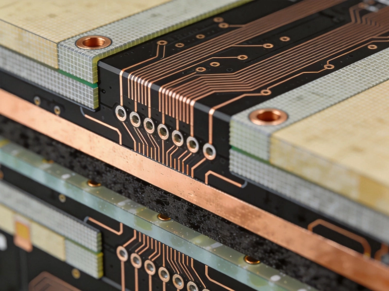
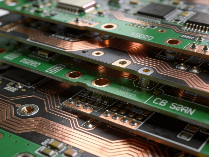
For double-sided and multilayer boards, multiple layers must be stacked and bonded together. This is where the term "Multilayer Pcb" comes from—boards with three, four, six, or even twenty-plus conducting layers.
The process starts with oxidation treatment of inner layer surfaces. This creates a microscopically rough texture that helps the layers bond properly. Each inner layer is then inspected and aligned using optical registration systems. Precision is critical here—misaligned layers result in faulty boards.
In the lamination press, layers stack together with prepreg (partially cured fiberglass sheets) between each copper layer. High temperature and pressure bond everything into a solid panel. The press applies forces typically around 300-400 PSI while heating to around 180°C. This "cooks" the board for a specific time, allowing the prepreg to fully cure and create strong mechanical bonds.
After lamination, the panel cools gradually to room temperature. Rushing this step can introduce stress and warpage into the board.
Drilling creates the holes that allow electrical connections between different layers. These include vias (vertical interconnect accesses) that connect traces on various layers, plus holes for through-hole components.
Chinese factories typically use computer-controlled drilling machines (CNC drilling or laser drilling) capable of drilling hundreds of holes per minute with micron-level precision. The drill bit size depends on the design—micro-vias might use laser drilling (0.1mm or smaller), while standard through-holes use mechanical drilling (0.2mm and up).
Drilling generates heat and pressure, so panels are often backed with aluminum or phenolic backup materials to prevent burring and reduce contamination. After drilling, a deburring process removes any raised copper edges around hole walls.
Critical parameters include hole position accuracy (typically within 0.05mm), wall roughness, and avoiding drill smear that could insulate the hole from the copper layer.
Freshly drilled holes have exposed fiberglass and resin, which don't conduct electricity. This step creates a thin conductive layer on the hole walls, establishing electrical connection between layers.
The process uses electroless copper deposition—a chemical autocatalytic process. Panels go through a series of cleaning, micro-etching, and catalyst application baths before entering the copper plating solution. The chemical reaction deposits a thin copper layer (typically 0.5-1.0 microns) on all exposed surfaces, including inside the holes.
After electroless plating, electroplating builds up the copper thickness. Panels are hung in a copper sulfate bath while electrical current attracts copper ions to the surfaces. This creates a thicker, more robust conductive layer inside holes—usually 20-25 microns for standard boards.
With the base structure complete, the outer copper layers receive their circuit patterns. This mirrors the inner layer process but operates on the board's exterior surfaces.
The panel gets coated with dry film resist, aligned with the outer layer artwork, and exposed to UV light. After developing, the pattern shows exactly where copper traces should remain. Then comes pattern plating—copper electroplating adds thickness to traces and the all-important barrel plating inside holes.
Tin or tin-lead plating follows copper plating. This metal acts as an etch resist, protecting underlying copper from the etchant during the next step. The tin plating must be uniform; inconsistent coverage leads to defective boards.
Stripping removes the photoresist, and etching removes exposed copper. Finally, another stripping process removes the tin plating, leaving behind the complete copper circuit pattern on the outer layers.
Solder mask is the green (or sometimes other colors) polymer layer that covers most of the board surface. It protects copper traces from oxidation, prevents solder bridges during assembly, and provides the characteristic green appearance most people associate with circuit boards.
Most modern factories use liquid photoimageable solder mask (LPI mask). This liquid gets applied by curtain coating, spray, or screen printing, then UV-cured. A solder mask film with openings for pads and holes is placed over the board and exposed. The exposed areas harden while unexposed areas wash away during development.
After development, the mask goes through final curing in an oven. The result is a durable, protective coating with precise openings that expose only the areas needing solder or component connection.
The exposed copper pads need protection from oxidation while remaining suitable for soldering. Surface finish options vary by application and cost considerations:
HASL (Hot Air Solder Leveling): The board gets dipped in molten solder, then hot air knives blow off excess, leaving a thin coating. This traditional finish offers good solderability but uneven surface quality, making it less suitable for fine-pitch components.
ENIG (Electroless Nickel Immersion Gold): A popular choice for advanced applications. A layer of nickel is deposited over the copper, followed by a thin gold layer. The nickel provides barrier protection while gold prevents oxidation. ENIG offers excellent flatness for BGA packages and fine-pitch components.
OSP (Organic Solderability Preservative): A water-based organic compound coats the copper surface, protecting it temporarily. This environmentally friendly option works well for lead-free processes but has limited shelf life.
Immersion Silver: Provides good flatness and solderability at moderate cost. Suitable for many applications but requires careful handling.
Hard Gold: For edge connectors and applications requiring repeated mating cycles. Uses thick gold plating over nickel underplate for wear resistance.
Silkscreen or legend printing adds component reference designators, logos, warning symbols, and other markings to the board surface. This helps assembly technicians place components correctly and aids in troubleshooting during and after manufacturing.
Modern factories typically use inkjet printing or direct legend printing (DLP) technology for higher precision and faster changeover times compared to traditional screen printing. The white or yellow ink used must withstand soldering temperatures without degrading.
The individual boards are cut out from the production panel. This step, called routing or depaneling, separates the panel into finished boards using one of several methods:
V-scoring: Partial cuts along the panel edges create weakened lines. Boards snap apart after manufacturing, offering a clean separation method for production panels.
NC Routing: Computer-controlled routers cut boards along programmed paths. This allows for complex board shapes and provides higher flexibility than V-scoring.
Laser Cutting: Used for very fine cuts or boards requiring minimal kerf loss. Offers high precision but slower processing speed compared to routing.
Punching: Using a die and press for high-volume production of simple rectangular boards. Fast and cost-effective for large runs but requires expensive tooling.
Every manufactured board undergoes electrical testing to verify functionality before shipping. This is non-negotiable—defective boards in customer products create costly problems.
Flying Probe Testing uses moving probes that touch test points on the board, checking for opens, shorts, and resistance values. This method suits low-to-medium volume production and prototypes without requiring expensive test fixtures.
Bed-of-Nails Fixture Testing uses a custom fixture with hundreds of spring-loaded pins contacting test points simultaneously. This enables faster testing for high-volume production runs where the fixture cost amortizes across many boards.
Most factories test 100% of boards for critical parameters: continuity (all traces properly connected), isolation (no unwanted connections between traces), and netlist verification (confirms the board matches the design connectivity).
Before shipping, boards receive final visual inspection. This includes checking for scratches, delamination, voids, registration accuracy, and solder mask quality. Many factories use automated visual inspection systems combined with human review for critical applications.
Boards are then packaged according to customer specifications. Common options include vacuum packaging with desiccant (to prevent moisture absorption), anti-static bags for ESD-sensitive boards, and custom trays or tubes for specific assembly requirements.
Documentation accompanies each shipment: Certificate of Conformance, test reports, dimensional reports, and material certifications depending on the board type and customer requirements.
China's dominance in Pcb Manufacturing stems from several compelling advantages:
Scale and Capacity: Chinese factories operate around the clock with massive production capacity. Whether you need 10 boards or 10 million, Chinese manufacturers can accommodate your volume.
Cost Efficiency: Labor costs, economies of scale, and the concentration of supply chains create significant cost advantages. Raw material suppliers, equipment manufacturers, and supporting services cluster near factory districts.
Technical Capability: Chinese manufacturers have invested heavily in advanced equipment and processes. Many produce HDI (High Density Interconnect) boards, flexible circuits, and ultra-fine line/space designs that rival any global competitor.
Speed: Quick-turn services offer prototype boards in 24-48 hours. Standard production runs often ship within 5-15 days depending on complexity and volume.
Supplier Ecosystem: From basic FR-4 to advanced Rogers materials, from standard finishes to specialized processes—Chinese suppliers offer comprehensive options under one roof.
While Chinese manufacturers offer many advantages, quality vigilance remains essential:
Request and verify certifications: ISO 9001, Iatf 16949 (automotive), UL listing, and RoHS compliance demonstrate commitment to quality systems and regulatory requirements.
Communicate specifications clearly: Provide complete Gerber files, drill files, stack-up information, and material requirements. Ambiguity leads to quality issues.
Start with prototypes: Test a small batch before committing to large orders. This validates the manufacturer's process capability for your specific design.
Consider inspection options: Many factories offer in-process inspection, AOI reports, or pre-shipment inspection services for an additional fee. For critical applications, these services provide valuable assurance.
The PCB fabrication process involves dozens of precise steps, each contributing to the board's final quality and reliability. From initial material preparation through drilling, plating, patterning, and testing, Chinese manufacturers have refined these processes over decades to deliver reliable products at competitive prices.
Understanding this process empowers you to make better sourcing decisions, communicate more effectively with manufacturers, and troubleshoot issues when they arise. Whether you're an engineer designing your first board or a procurement professional managing supply chains, this knowledge proves valuable across the electronics industry.
Chinese PCB factories continue advancing their capabilities, investing in automation, better process control, and higher technology boards. As the electronics industry evolves—toward smaller devices, faster frequencies, and more complex systems—Chinese manufacturers adapt alongside it, ensuring they remain essential partners in global electronics production.
How to Reduce Your PCB Manufacturing Costs Without Sacrificing QualityJuly/08/2026
PCB Assembly Price China: A Complete Cost Guide for 2024May/18/2026
Understanding PCB Assembly Prices in China: What Factors Influence Cost?June/10/2026
What is a Multilayer PCB? A Comprehensive Guide for EngineersJuly/02/2026
Thru-Hole vs. SMT: Choosing the Right Assembly Technology for Your PCBJuly/10/2026
Understanding HDI PCB Technology: A Comprehensive Guide for BeginnersMay/13/2026
How HDI PCBs Enable Slimmer Smartphones and TabletsJune/26/2026
Top 10 DFM Tips to Avoid Errors in Your Next PCB OrderJune/18/2026