Open Nav

Surface Mount Technology (SMT) has dominated Electronics Manufacturing for decades, yet improper pad design remains one of the leading causes of assembly defects and field failures. Getting SMT pad design right isn't complicated, but it requires understanding the relationship between component packages, soldering physics, and manufacturing tolerances. This guide covers the essential considerations every PCB designer needs to know.
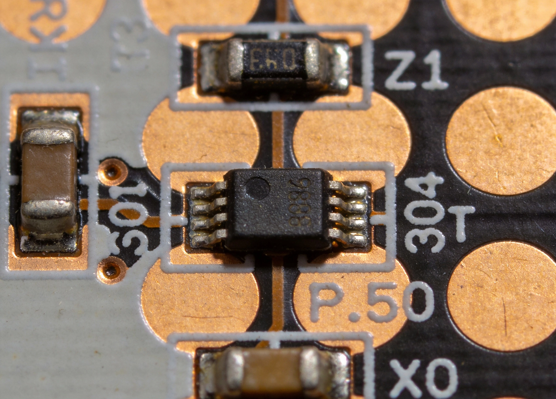
The solder joint is the mechanical and electrical connection between component and board. Poor pad design creates joints that are either too weak (insufficient solder volume or coverage) or too stressed (excess solder causing tombstoning or cracking). Either failure mode shortens product lifespan and increases warranty costs.
Beyond reliability, pad design affects manufacturing yield. Boards that require excessive rework consume labor and introduce human error. Designs optimized for assembly flow faster through production, reducing per-unit cost and time to market. Understanding pad design fundamentals pays dividends across the entire product lifecycle.
SMT pad size involves three dimensions: length (in the direction of component placement), width (perpendicular to placement direction), and spacing (center-to-center distance between pads for multi-pin packages). Each dimension affects solder joint formation differently, and all three must be optimized together.
Pad length extends beyond the component termination on each side, providing wetting surface for solder to climb up the component body. Pad width must accommodate the component termination width plus manufacturing tolerance. Too narrow creates alignment problems; too wide wastes board space and can cause adjacent pad bridging.
Most SMT pad design follows either Ipc Standards or manufacturer recommendations. IPC-7351 (Generic Requirements for Surface Mount Design and Land Pattern Standard) provides generic land pattern geometries based on component dimensions and expected manufacturing capability. These standards balance component packing density against assembly yield.
Component manufacturers often publish recommended land patterns based on their specific termination dimensions and expected solder joint geometry. When available, these manufacturer recommendations should override generic IPC calculations—they account for component-specific characteristics that generic standards cannot address.
The general principle: pad dimensions should be slightly larger than the component terminations they receive. For most chip components (resistors, capacitors), IPC recommends adding approximately 0.1mm to 0.3mm per side to termination dimensions, scaling up for larger packages and down for smaller ones.
Component spacing affects both assembly yield and board density. Minimum spacing requirements depend on component heights, placement accuracy, and whether reflow or hand assembly is intended. For automated assembly with standard placement equipment, minimum spacing typically ranges from 0.2mm to 0.5mm depending on component sizes.
Taller components next to shorter ones create shadowing during reflow—the taller part blocks radiant heat from reaching solder paste on adjacent components. This can cause incomplete solder joints. Maintain at least 2x the height difference as spacing between components, or design thermal profiles to account for shadowing effects.
Components generate heat during operation, and they also dissipate heat differently based on their surroundings. Dense packing of power components creates thermal interaction that may affect both performance and reliability. Leave adequate spacing around components that dissipate significant power, or design Thermal Management features to handle the combined heat load.
Thermal relief connections to planes should maintain adequate spacing from other pads to prevent heat sinking during soldering. If a pad is too well connected to a large copper plane, the plane acts as a heat sink during reflow, preventing the pad from reaching reflow temperature. Use thermal relief spokes rather than solid connections when pads must connect to large planes.
Multi-pin packages (QFN, BGA, SOIC, etc.) require routing channels between pads. Plan your fanout strategy early—changing routing after component placement is painful and often impossible without major rework. Understand your PCB manufacturer's Minimum Trace Width and spacing capabilities when designing fanout patterns.
For fine-pitch packages, vias-in-pad or dog-bone fanout structures are common. Each approach has tradeoffs: vias-in-pad provide shortest routing but complicate assembly; dog-bone structures are more forgiving but require more board area. Choose based on your density requirements and manufacturing capabilities.
Consistent component orientation improves assembly efficiency and reduces errors. Industry convention orients components with pin 1 at a standardized position—for most packages, pin 1 starts at the top-left when viewing the board from the top side. Following this convention helps assembly operators quickly identify pin 1 for polarized components.
For packages with genuine polarity (diodes, LEDs, electrolytic capacitors, ICs with pin 1 marking), maintain consistent orientation across the board. This makes visual inspection faster and helps troubleshooting. When packages have mechanical polarization (keys, notches, beveled corners), orient them consistently to match the standard marking conventions.
Component orientation affects placement speed. Standard SMT placement equipment is fastest when placing components in consistent directions—components all oriented the same way or in 90-degree increments following a logical pattern. Some designers rotate components to align with signal flow or board shape, but this can slow assembly.
For high-volume production, consult your assembly house about optimal orientation patterns. Many shops can optimize placement programs for speed, but providing a board designed with assembly flow in mind costs nothing and may reduce per-unit assembly time.
Silkscreen markings clearly indicate component designators, polarity, and pin 1 location. These markings survive into production and field service, providing critical reference for assembly, inspection, and repair. Include pin 1 dots or chamfered corner indicators for all polarized packages, even if the component body has molded polarity marks.
Silkscreen text should be readable and appropriately sized—at least 1mm character height for designators, with clear polarity symbols for diodes, LEDs, and capacitors. Avoid placing silkscreen markings under components where they would be covered; the markings should be visible after assembly for service technician reference.
Chip components (0201, 0402, 0603, 0805, etc.) require careful pad sizing because their small size makes alignment critical. For 0402 and smaller, Ipc Standards suggest approximately 0.4mm pad width with 0.4mm spacing for typical applications. Larger chip sizes scale proportionally.
Tighter tolerances (medical, aerospace, automotive) often require smaller pads to reduce solder joint volume and improve placement accuracy feedback. Less precise applications can use larger pads for manufacturing margin. Match pad size to your application requirements rather than blindly following maximum density recommendations.
Quad Flat No-lead (QFN) and Dual Flat No-lead (DFN) packages present unique challenges because their leads are hidden beneath the package body. These packages rely on thermal pads or ground pads under the body for Heat Dissipation and often for electrical grounding.
Thermal pad design requires via arrays for heat transfer to internal planes. Without adequate thermal vias, the device overheats and fails prematurely. Include thermal vias on approximately 1mm pitch under the exposed thermal pad, connected to appropriate planes. The vias should be solder-mask defined (smaller mask opening than copper) to prevent solder wicking.
Ball Grid Array (BGA) packages require careful consideration of ball pitch, ball diameter, and routing strategy. PCB manufacturers publish capability charts for Minimum Trace Width, spacing, and via size at various BGA pitches. Design your fanout to match manufacturer capabilities from the start.
BGAs require either Microvias for fine-pitch routing or dog-bone fanout structures that route traces to vias outside the BGA footprint. Microvia Technology (laser-drilled Blind Vias) provides the highest density but increases manufacturing cost. Dog-bone fanout works with standard through-hole vias but requires more board area.
More pad is not always better. Excessively large pads cause tombstoning (component stands up on end during reflow) because they heat faster than the component termination, creating surface tension imbalance. Large pads also waste board space and can cause bridging between adjacent pads if paste deposition isn't carefully controlled.
The fix is straightforward: use IPC-7351 calculations or manufacturer recommendations, and avoid inflating dimensions "just to be safe." Modern solder paste and reflow profiles handle standard pad sizes reliably. Only increase pad size when you have documented evidence of assembly problems.
Solder mask defines where solder can and cannot flow. If mask clearance is too small, solder bridges form between adjacent pads. Standard practice maintains mask web of at least 0.1mm to 0.15mm between adjacent pads. For fine-pitch packages, this may require solder-mask defined (SMD) pads where the mask opening is smaller than the copper pad.
Non-solder-mask-defined (NSMD) pads provide better mechanical adhesion between copper and mask, but SMD pads provide better control of solder placement. Choose based on your package and reliability requirements—NSMD is generally preferred for fine-pitch packages where pad position tolerance is critical.
Pads connected to large copper planes without thermal relief create assembly nightmares. The plane acts as a heat sink, preventing the pad from reaching reflow temperature. Components near thermal pads may never solder properly. Always use thermal relief spokes connecting pads to planes—typically four spokes of appropriate width for the pad size.
The exception is thermal pads for power components where maximum heat transfer is required. For these pads, full connection to the plane is intentional, and assembly process is adjusted (pre-heating, longer soak time) to ensure reliable solder joints despite the thermal mass.
Even if you design for in-circuit test, accessible test points improve debug and repairability. Include test points for critical nets, particularly power and ground connections, signal inputs/outputs, and firmware programming connections. Via test points are cheap but valuable—add them during layout rather than retrofitting later.
Test points should be at least 1mm diameter for probe accessibility, positioned away from component bodies and other test points. Four-wire Kelvin test points provide most accurate resistance measurements for current sensing or high-precision circuits.
Components that cannot be visually inspected (BGAs, QFNs with bottom-terminations) require X-ray Inspection capability. Design your board with X-ray access in mind—avoid placing metal features (heatsinks, shields, ground planes) directly under packages that require inspection.
Automated Optical Inspection (Aoi) requires component presence and orientation verification. Ensure component body colors contrast with board silkscreen, and avoid placing components on top of silkscreen markings. Aoi cameras need clear visibility of component edges and terminations.
Successful SMT design balances multiple competing requirements: manufacturability, reliability, density, and testability. Pad sizes should follow IPC standards or manufacturer recommendations rather than arbitrary inflation for "safety." Component spacing must accommodate placement accuracy, thermal interactions, and routing needs. Orientation conventions improve assembly efficiency and reduce errors.
Package-specific considerations require attention to thermal pad design, fanout strategies, and inspection requirements. BGA and QFN packages demand more planning upfront but reward careful design with reliable products. Avoid common mistakes like oversized pads, insufficient mask clearance, and missing thermal relief.
Validate your design through Dfm (Design For Manufacturability) review with your assembly house before releasing to production. Many problems are cheaper to fix on paper than after fabrication. Building prototypes with the intended assembly process catches remaining issues before committing to volume production.
What pad size should I use for 0402 resistors?
Per IPC-7351, recommended pad dimensions for 0402 are approximately 0.55mm length and 0.5mm width. Many manufacturers recommend slightly larger pads (0.6mm x 0.55mm) for improved manufacturability.
How close can I place SMT components?
Minimum spacing depends on component height and assembly capability. A safe minimum is 0.2mm to 0.3mm for adjacent 0402/0603 components, scaling up based on relative heights and thermal considerations.
Should I use SMD or NSMD pads?
NSMD (Non-Solder-Mask-Defined) pads are generally preferred for fine-pitch components where precise pad geometry matters. SMD (Solder-Mask-Defined) pads provide better solder bridging control for larger components or packages with tight thermal cycling requirements.
How many thermal vias do I need for a QFN thermal pad?
A typical QFN thermal pad needs 8 to 16 thermal vias on approximately 1mm pitch. The exact number depends on power dissipation requirements and thermal plane design. More vias improve thermal performance but may complicate manufacturing.
Why does my board have tombstoning problems?
Tombstoning typically results from uneven heating or oversized pads. Ensure both pads of a component reach reflow temperature simultaneously, and check that pad sizes follow IPC recommendations rather than being unnecessarily large.

The Complete Guide to SMT PCB Assembly in ChinaJune/17/2026

BGA Assembly Challenges: X-Ray Inspection and Voiding IssuesSeptember/17/2026

SMT PCB Assembly China: A Complete Guide for Global BuyersMay/18/2026

Top 10 DFM Mistakes to Avoid Before Sending Files to China for SMT AssemblyJuly/15/2026

Emergency PCB Runs: Can Chinese Manufacturers Meet Tight Deadlines?August/14/2026

What to Look for in a Reliable SMT PCB Assembly Partner in ChinaAugust/10/2026

The Rise of Flexible PCBs in Foldable Phone HingesJuly/14/2026

Turnkey PCB Assembly: Simplifying Your Supply Chain with One VendorOctober/10/2026