Open Nav

In the fast-paced world of Electronics Development, speed can make or break a product launch. Whether you are an independent hardware startup racing against competitors or an engineering team prototyping the next generation of IoT devices, waiting weeks for PCB samples simply is not an option anymore. That is why 24-hour Pcb Prototyping has become a critical service for engineers who need to validate designs, test iterations, and move from concept to functional prototype in the shortest time possible.
But what does it actually take to turn a set of Gerber files into finished, high-quality circuit boards in just 24 hours? The answer lies not in cutting corners, but in building a highly optimized manufacturing pipeline that eliminates waste at every stage. In this article, we will walk you through our complete process—from the moment you upload your Gerber files to the day your PCBs arrive at your doorstep.
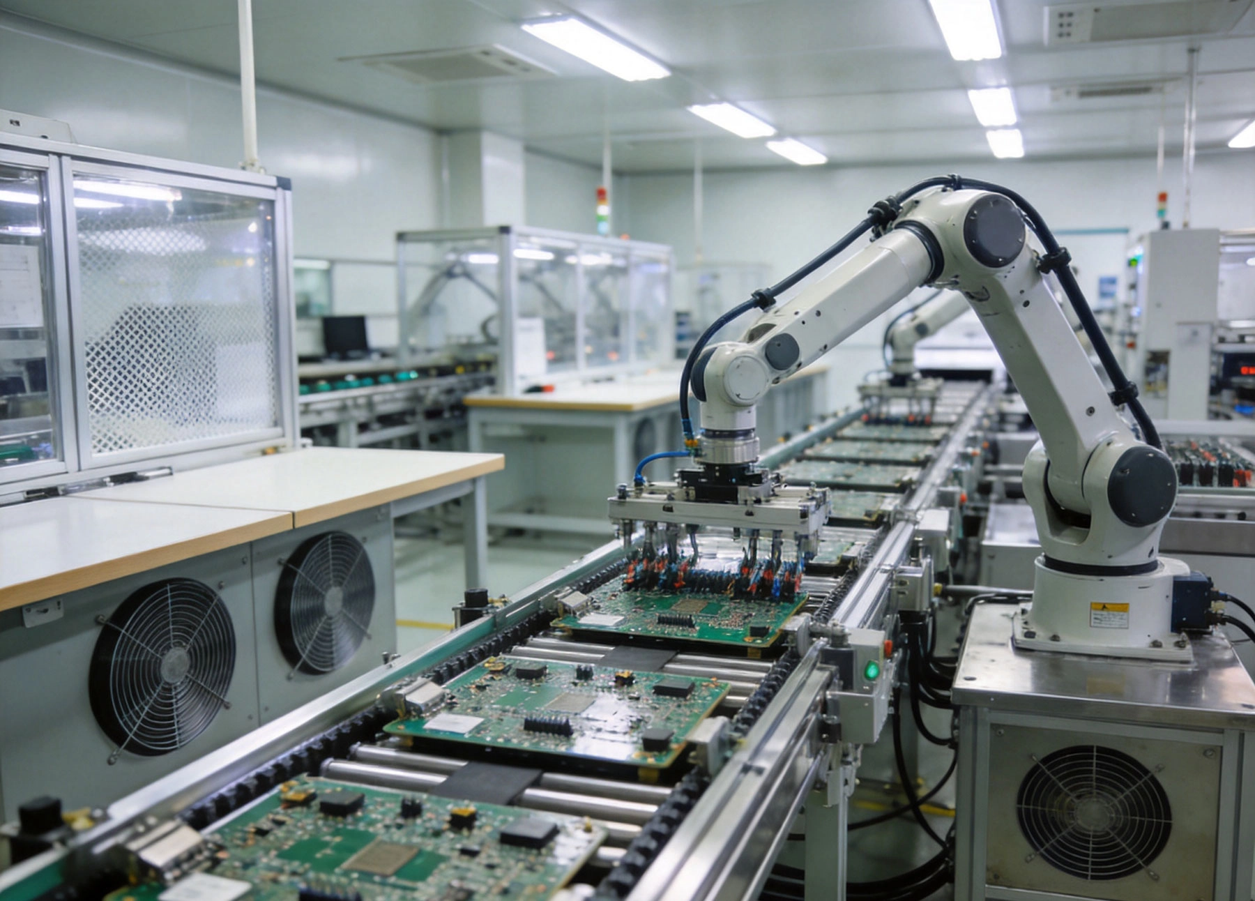
Time-to-prototype is one of the most significant bottlenecks in hardware development. Traditional Pcb Manufacturing lead times range from 5 to 15 business days, which can stretch into weeks when shipping and customs are factored in. For engineers working on iterative designs, each week of waiting means slower learning cycles, delayed feedback, and ultimately a longer path to market.
24-hour Pcb Prototyping compresses this timeline dramatically. When you can receive your first prototype within a single day, you can test your assumptions in real time, identify design flaws before they become expensive problems in production, and ultimately ship your final product faster. The ability to iterate daily rather than weekly is a genuine competitive advantage in today's electronics landscape.
Every successful 24-hour Pcb Prototype begins before manufacturing even starts—with your Gerber files. These files are the universal output from nearly all Pcb Design software, containing all the copper traces, drill holes, solder masks, and silkscreen layers that define your board. The accuracy of your Gerber files directly determines how smoothly the rest of the process will go.
We strongly recommend running a Design Rule Check (DRC) in your CAD software before exporting your files. This automated check validates your design against manufacturing constraints such as Minimum Trace Width, spacing between traces, and drill hole sizes. Catching these issues in the design phase prevents costly re-spins that would blow past your 24-hour target. We also accept a range of file formats including Gerber X2, which includes additional metadata that helps our CAM team process your boards more accurately.
Once your Gerber files arrive in our system, they enter our automated CAM (Computer-Aided Manufacturing) processing pipeline. This is where the magic of speed begins. Our software automatically parses your Gerber files and performs initial validation, checking for common issues like missing drill files, mismatched layer counts, or aperture mismatches.
For standard PCB prototyping orders, this automated process handles the vast majority of cases without human intervention. The system generates the machine programs for our CNC drilling machines, selects the appropriate tooling, and calculates the optimal routing paths for Panelization. This automation alone eliminates hours that would otherwise be spent on manual file processing.
However, our experienced CAM engineers are always standing by for complex orders. If your design includes advanced features like blind/Buried Vias, Controlled Impedance traces, or non-standard board shapes, our team steps in to manually optimize the manufacturing data. This hybrid approach—automation for routine cases, expert review for complex ones—ensures both speed and quality across all orders.
With manufacturing data finalized, we move into board preparation. For most 24-hour prototyping orders, we use our stocked inventory of premium substrate materials. This includes standard FR-4 in various thicknesses (0.4mm to 3.2mm), high-Tg alternatives for demanding thermal environments, and Flex Pcb materials for applications that require bending or folding.
Having these materials pre-stocked is essential for achieving 24-hour turnaround. Unlike Mass Production orders where we might optimize for material cost, prototyping orders prioritize availability and speed. We maintain buffer stocks of the most commonly requested materials so that we can begin processing your order immediately without waiting for material deliveries.
For boards requiring specialty materials—such as Rogers high-frequency laminates for RF applications or metal-core substrates for high-power LED designs—our team will communicate with you about realistic lead times, as these materials may require additional sourcing time that extends beyond the standard 24-hour window.
With materials ready and manufacturing data loaded, the actual fabrication begins. Our standard 24-hour PCB prototyping service covers the following core processes, all completed within a single production shift:
For multilayer boards (4 layers and above), we begin with inner layer processing. The copper-clad laminate is cleaned and coated with photoresist, then exposed to UV light using your Gerber-defined artwork. After development and etching, we have the inner layer patterns ready. Automated Optical Inspection (Aoi) verifies that the etched patterns match your original design, catching any defects before the layers are laminated together.
The processed inner layers are stacked with prepreg (partial-cure fiberglass sheets) and outer copper layers, then laminated under high pressure and temperature. This step bonds all the layers into a solid board and cures the prepreg to its final rigid state.
Via formation happens next. We drill all through-holes and micro-vias according to the drill files generated during CAM processing. For multilayer boards, we also perform Sequential Lamination and drilling for any blind or Buried Via structures. After drilling, the holes are chemically cleaned and electroless copper plating deposits a thin conductive layer on the hole walls, creating the electrical connections between layers.
The outer layers are imaged and plated to create the final copper traces specified in your design. The board is then coated with solder mask—typically green, though we offer a variety of colors for prototyping orders. The solder mask protects the copper traces while leaving the pads exposed for component assembly. Finally, surface finishes are applied: Hasl (Hot Air Solder Leveling), Enig (Electroless Nickel Immersion Gold), or Osp (Organic Solderability Preservative) depending on your assembly requirements.
One of the most common concerns about fast-turn Pcb Manufacturing is whether quality suffers. This is a legitimate concern, and we take it seriously. Our 24-hour prototyping service maintains the same rigorous quality standards as our standard production service, but with parallel processing to minimize delays.
Every board goes through a combination of automated and manual inspection processes. Flying probe testing checks electrical connectivity between all nets on the board, verifying that there are no opens or shorts. For boards with high layer counts or complex routing, we supplement flying probe testing with cross-sectional analysis on sample boards to verify via quality and plating thickness. Our quality team also performs visual inspection under magnification to catch any cosmetic defects that might affect assembly.
We track defect rates as a key performance metric across all our services. Our 24-hour prototyping service maintains a first-pass yield rate above 98%, and any boards that do not pass inspection are reworked or remade at no additional cost to you. You should receive fully functional boards that are ready for assembly.
After testing, the individual boards are routed out of the production panel using precision CNC milling. This profiling step cuts the boards to their final dimensions and creates any special shapes specified in your design files. V-scoring is available for panels with multiple boards, making it easier to depanelize them after assembly.
Once the boards are finished and inspected, they are packaged with anti-static materials and prepared for shipping. We partner with major express carriers to offer global delivery, including expedited options for destinations that are farther from our manufacturing facilities. For most locations in Asia, Europe, and North America, express shipping delivers your boards within 1 to 3 business days after they leave our facility.
While our manufacturing pipeline is optimized for speed, there are several things you can do on your end to ensure your order arrives within 24 hours:
Our 24-hour service serves a wide range of industries and applications. Hardware startups use it to validate their MVP designs before seeking seed funding. Academic research teams rely on it for lab experiments where waiting weeks for samples would derail research timelines entirely. Embedded systems engineers use it to debug firmware on real hardware rather than relying solely on simulation. Even large enterprises use 24-hour prototyping for emergency replacement boards when production equipment fails unexpectedly.
The common thread across all these use cases is the need for speed combined with reliable quality. When you are iterating on a design, the value of fast feedback cannot be overstated. Catching a trace width error or an incorrect pinout in your first prototype rather than your fifth iteration saves days of engineering time and thousands of dollars in development costs.
Our standard 24-hour service accommodates boards up to 400mm x 500mm (approximately 15.7" x 19.7"). For larger boards or non-standard dimensions, please contact our team to discuss feasibility and adjusted lead times.
We support 1 to 16 layer boards in our standard 24-hour service. Standard stack-ups using FR-4 materials process fastest. Higher layer counts and specialty configurations may require additional verification time.
Simple flexible circuits with single-sided or double-sided designs may qualify for 24-hour turnaround on a case-by-case basis. Complex multilayer rigid-flex boards typically require 48 to 72 hours due to the additional lamination steps involved.
We accept Gerber files (RS-274X and Gerber X2), as well as ODB++ and Eagle XML export formats. For best results, export your files with full design metadata included.
Yes. Every board undergoes flying probe testing, and we provide a basic test report showing net connectivity upon request. Detailed test reports with high-resolution imagery are available for a small additional fee.
24-hour PCB prototyping is not just about running machines faster—it is about building a smarter manufacturing system that eliminates waste, automates routine decisions, and keeps experienced engineers focused on the cases that need human judgment. From the moment your Gerber files enter our system to the day your boards arrive, every step is designed to maximize efficiency without sacrificing the quality your products depend on.
If you have a design ready and need prototypes fast, upload your Gerber files today and select our 24-hour turnaround option. Our team is ready to help you move from concept to functional hardware faster than you thought possible.
This article is provided for informational purposes and reflects our general experience with PCB prototyping processes. Specific capabilities and turnaround times may vary based on order volume and material availability.

The Logistics of Fast Shipping: Getting Your PCBs from China QuicklySeptember/16/2026
Speeding Up Product Development with Fast PCB Prototype ServicesJuly/27/2026
Why Low Volume PCB Manufacturing is Crucial for Agile Hardware DevelopmentOctober/16/2026
Low Volume PCB Manufacturing: Ideal Solutions for Startups and R&DOctober/08/2026
Metal Core PCB (MCPCB) Basics: Aluminum vs. Copper SubstratesSeptember/29/2026
How to Design High-Layer Count PCBs (20+ Layers) for Complex ElectronicsSeptember/08/2026
Preparing Your Gerber Files for a Smooth China PCB Fabrication ProcessSeptember/18/2026
The Rise of Flexible PCBs in Foldable Phone HingesJuly/14/2026