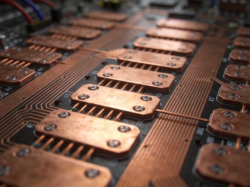
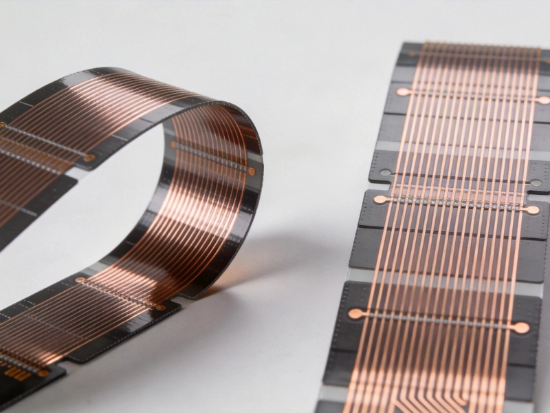
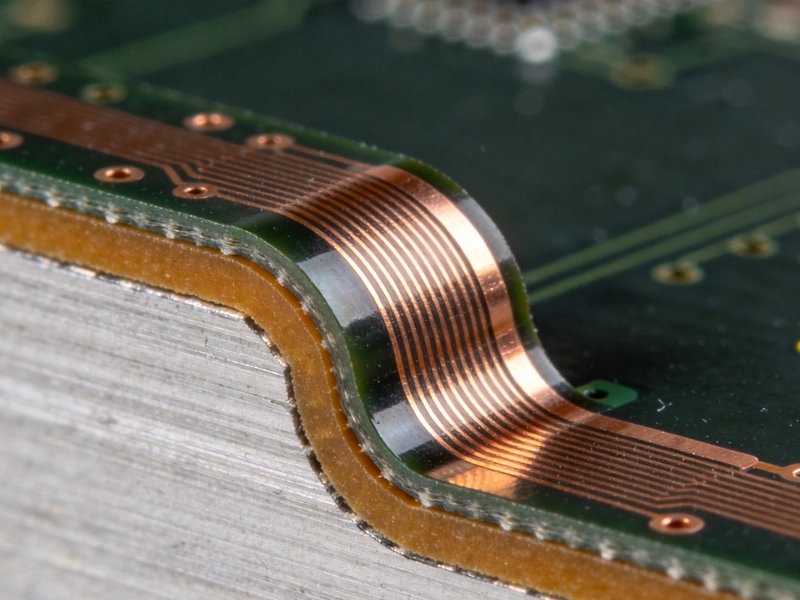
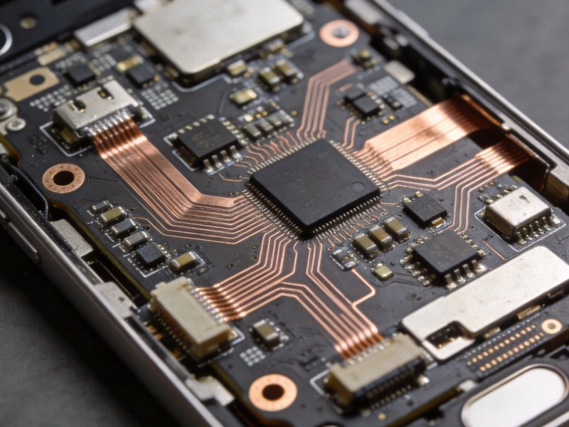
Heavy copper PCBs represent the go-to solution for power-critical applications requiring high Current Carrying Capacity and exceptional Thermal Management. If you've ever wondered how industrial motor controllers handle hundreds of amps without overheating, how power converters maintain efficiency under full load, or how battery management systems dissipate heat from high-current paths, the answer lies in heavy copper Pcb Technology.
As a China Heavy Copper Pcb manufacturer with 18+ years of experience in Power Electronics applications, we've produced millions of heavy copper boards ranging from 3 oz to 20 oz thickness for industries worldwide. This comprehensive guide explains everything you need to know about heavy copper PCBs, from Copper Thickness standards and current capacity calculations to design considerations and manufacturing processes.

What is a Heavy Copper PCB?
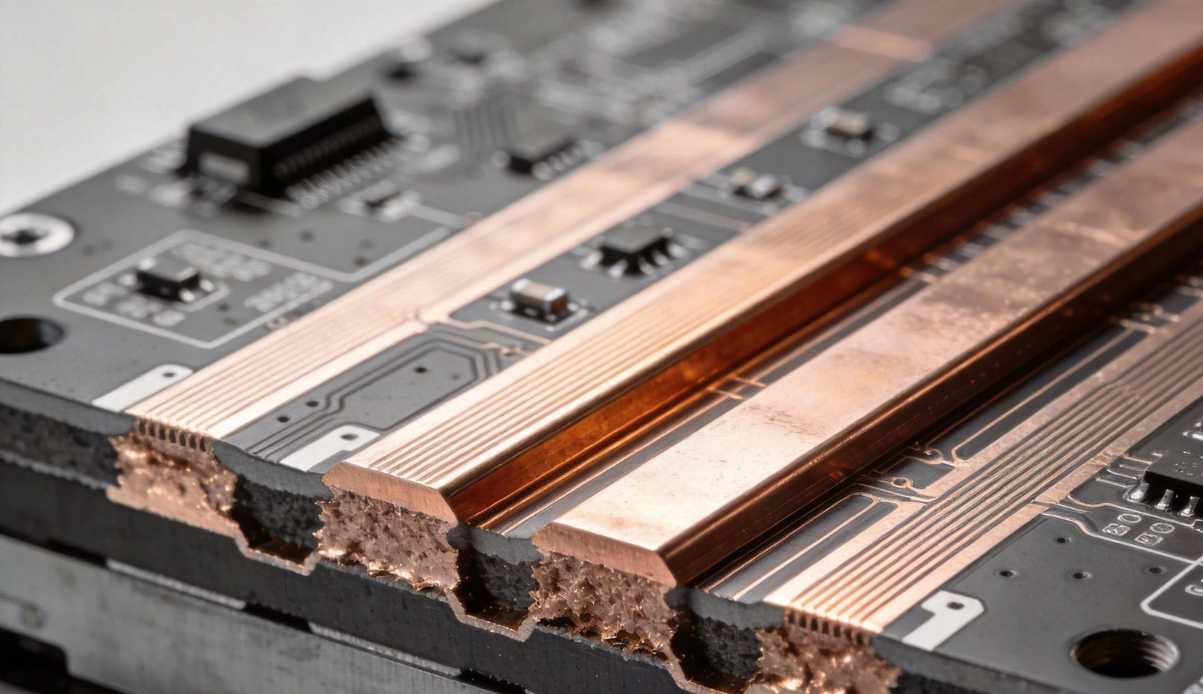
A Heavy Copper Pcb is a Printed Circuit Board with Copper Thickness significantly exceeding standard PCB specifications. While standard PCBs typically use 1 oz (35μm) copper thickness for signal layers and 2 oz (70μm) for power layers, heavy copper PCBs feature copper thicknesses starting at 3 oz (105μm) and extending to 20 oz (700μm) or even thicker for specialized applications.
The defining characteristic of heavy copper PCBs is their ability to carry high currents with minimal temperature rise. The thicker copper provides lower electrical resistance, which translates directly to lower power loss, reduced heat generation, and improved overall efficiency for power-critical applications.
Heavy copper Pcb Technology has been refined over decades, with applications expanding from industrial motor controls to include power converters, battery management systems, renewable energy equipment, and electric vehicle Power Electronics. Modern heavy copper PCBs can achieve copper weights up to 40 oz (1,400μm) in some specialized applications.
Heavy Copper Thickness Standards
Heavy copper PCBs are categorized by their copper thickness, commonly expressed in "ounces" (oz) based on the weight of copper per square foot. The relationship between ounces and micrometers:
-
Standard copper: 1 oz (35μm), 2 oz (70μm)
-
Heavy copper starts: 3 oz (105μm)
-
Medium-heavy copper: 4-6 oz (140-210μm)
-
Heavy copper: 8-12 oz (280-420μm)
-
Extreme copper: 15-20 oz (525-700μm)
-
Ultra-heavy copper: 30+ oz (1,050μm+)
Thickness selection depends on current carrying requirements, board size constraints, thermal performance needs, and manufacturing cost considerations. In our experience, 3-4 oz copper handles most medium-power applications (up to 10-15A), 6-8 oz handles high-power applications (15-30A), and 12+ oz handles extreme current requirements (30A+) in space-constrained designs.
Current Carrying Capacity
The primary advantage of heavy copper PCBs is their ability to carry high currents with minimal temperature rise. Current Carrying Capacity depends on several factors:
Copper Thickness
Thicker copper provides larger cross-sectional area for current flow, reducing resistance and enabling higher current capacity. General current capacity guidelines (single trace, 10°C temperature rise):
-
3 oz (105μm): ~10-12A for 2mm trace width
-
4 oz (140μm): ~15-18A for 2mm trace width
-
6 oz (210μm): ~22-28A for 2mm trace width
-
8 oz (280μm): ~30-38A for 2mm trace width
-
12 oz (420μm): ~45-60A for 2mm trace width
-
20 oz (700μm): ~75-100A for 2mm trace width
These values increase with wider trace widths and decrease with tighter spacing and higher ambient temperatures. Our engineering team provides detailed current capacity calculations for every design based on exact trace geometries, board layout, and operating conditions.
Trace Width and Spacing
Wider traces provide larger cross-sectional area, increasing current carrying capacity. However, design rules require specific spacing between traces based on voltage isolation requirements. Heavy copper PCBs typically use:
-
Power traces: 2-10mm wide depending on current requirements
-
Spacing: 0.5-2mm depending on voltage differential and isolation requirements
-
Vias: Multiple vias or large via barrels needed for heavy copper current transfer
Our standard design rules include specific width and spacing recommendations for each copper thickness to ensure manufacturability and reliability.
Temperature Rise
Heavy copper PCBs are designed for low temperature rise even under high current loads. The standard design approach targets maximum temperature rise of 10-20°C under maximum continuous load. This conservative approach ensures reliability and longevity. For applications requiring even lower temperature rise, heavier copper or additional Thermal Management strategies may be needed.
Key Benefits of Heavy Copper PCBs
1. High Current Carrying Capacity
The defining advantage of heavy copper PCBs is their ability to handle high currents without excessive heating:
-
Support currents from 10A to 100A+ depending on copper thickness and trace design
-
Low resistance reduces power loss and improves efficiency
-
Consistent performance across wide load ranges without thermal derating
-
Reduced need for external bus bars or power cables in many applications
For industrial motor controllers, heavy copper PCBs enable compact designs that eliminate external wiring for power distribution. We've designed 48V motor controllers handling 100A continuous current using 8 oz copper on a 4-layer board, with no external bus bars required.
2. Superior Thermal Management
Heavy copper PCBs provide excellent thermal management:
-
Thick copper spreads heat efficiently, preventing hot spots
-
Higher thermal conductivity compared to standard copper thicknesses
-
Enables higher component density by managing heat from power devices
-
Reduces need for additional heat sinks and thermal management components
In battery management systems for electric vehicles, heavy copper PCBs help maintain optimal cell temperatures by efficiently spreading heat across the board surface, improving battery pack performance and longevity.
3. Enhanced Mechanical Strength
The thick copper layers provide significant mechanical advantages:
-
Stiffness: Heavy copper layers increase board stiffness, reducing bending and warping
-
Thermal expansion: Reduced thermal expansion mismatch between copper layers and FR-4 substrate
-
Vibration resistance: Heavy copper improves resistance to vibration-induced failures
-
Impact resistance: More resistant to damage from handling and assembly processes
Automotive heavy copper PCBs must survive 10+ years under harsh conditions including temperature cycling, vibration, and mechanical stress. The heavy copper construction helps meet these demanding reliability requirements.
4. Improved Reliability and Longevity
Lower operating temperatures and reduced stress contribute to improved reliability:
-
Lower temperatures reduce component degradation rates
-
Reduced thermal cycling stress on solder joints and components
-
Consistent electrical performance over product lifetime
-
Extended product lifetimes with reduced field failures
For industrial applications with 20+ year expected lifetimes, heavy copper PCBs provide the reliability margin needed to meet customer expectations while reducing
Total Cost Of Ownership.
5. Design Flexibility
Heavy copper PCBs support complex power system designs:
-
Integration of power and control circuitry on single board
-
Multi-layer designs with heavy copper on power layers and standard copper on signal layers
-
Controlled Impedance for high-speed signals alongside power circuits
-
Complex ground plane structures for EMI management
This integration capability enables compact designs that would require multiple separate boards using conventional approaches, reducing assembly complexity and improving reliability.
Common Applications of Heavy Copper PCBs
Power Electronics and Converters
Heavy copper PCBs are essential for high-power electronics:
-
Power supplies: Switching power supplies, DC-DC converters, AC-DC power supplies—handle high currents efficiently
-
Motor controllers: Variable frequency drives (VFDs), servo drives, motor controllers—manage motor phase currents
-
Inverters: Solar inverters, grid-tie inverters, motor drive inverters—handle high-current switching
-
Battery chargers: Fast chargers for EVs, industrial battery chargers—manage high charge currents
We produce heavy copper PCBs for power electronics up to 10kW power levels using 8-12 oz copper with minimal external power distribution hardware.
Automotive Electronics
Automotive applications demand high reliability under harsh conditions:
-
Battery management systems: High-current cell balancing and monitoring
-
Power distribution modules: Handle vehicle electrical distribution currents
-
Motor controllers: Electric vehicle motor drives and converters
-
Lighting systems: High-power LED and xenon lighting power distribution
All automotive heavy copper PCBs we produce meet
Iatf 16949 automotive quality requirements and are qualified for 125°C operating temperatures with vibration resistance testing.
Industrial Automation and Control
-
Motor drives: Industrial motor controllers and variable frequency drives
-
Power distribution: Industrial power supplies and distribution panels
-
Welding equipment: Arc welding and resistance welding power controllers
-
Test equipment: High-power test and measurement equipment
Industrial heavy copper PCBs must survive harsh environments with dust, chemicals, temperature extremes, and long operating lifetimes. The heavy copper construction provides inherent advantages for these demanding applications.
Renewable Energy Systems
-
Solar inverters: High-power DC-AC conversion for photovoltaic systems
-
Wind turbine converters: Power electronics for wind energy systems
-
Energy storage systems: Battery management and power conversion for energy storage
-
Grid integration: Power electronics for renewable energy grid connection
Renewable energy applications require reliability and efficiency for 20+ year operational lifetimes. Heavy copper PCBs help achieve these requirements through robust construction and excellent thermal management.
Electric Vehicle Systems
-
Motor controllers: High-power motor drives for electric and hybrid vehicles
-
Battery management: High-current cell monitoring and balancing
-
On-board chargers: High-power battery charging systems
-
Power distribution: Vehicle high-voltage power distribution
Heavy Copper PCB Manufacturing Process
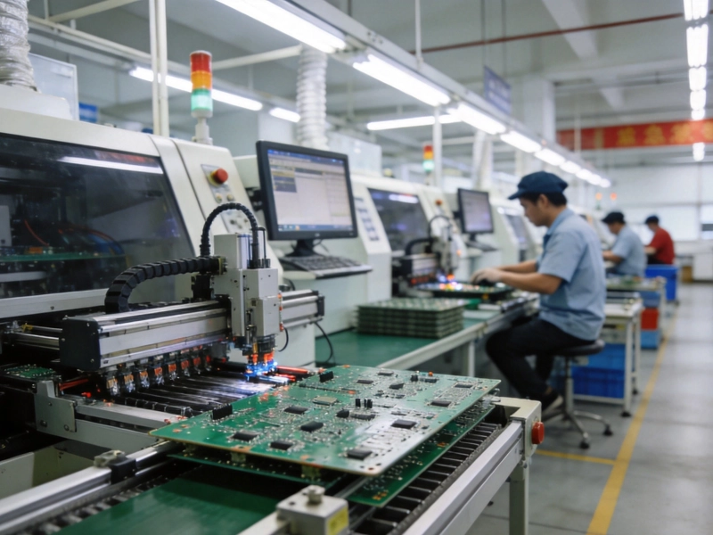
Heavy copper Pcb Manufacturing requires specialized processes for handling thick copper:
-
Material preparation: FR-4 cores prepared for heavy copper lamination
-
Heavy copper lamination: Thick Copper Foil (3-20+ oz) laminated to FR-4 cores under high pressure and temperature
-
Circuit imaging: Photoresist applied, exposed through circuit artwork, and developed
-
Etching: Unprotected copper etched away—thicker copper requires longer etch times and precise control
-
Drilling: Through-holes drilled—larger drill bits needed for via barrels accommodating heavy copper
-
Plating: Desmear treatment followed by electroless and electrolytic copper plating
-
Outer layer processing: Additional heavy copper layers added for multi-layer designs
-
Solder mask and surface finish: Protective coatings applied
-
Electrical testing: 100% electrical testing verifies continuity and isolation
-
Current capacity testing: Sample boards tested to verify current carrying capacity under load
-
Final inspection: Thickness measurements, visual inspection, quality verification
For multi-layer heavy copper PCBs, special attention is paid to copper thickness consistency across all layers and proper registration between layers to ensure uniform electrical performance.
Design Guidelines for Heavy Copper PCBs
Current Capacity Calculation
Calculate required current capacity for each power trace:
-
Determine maximum continuous current for each power path
-
Select copper thickness based on current requirements and space constraints
-
Calculate required trace width: W = I / (K × ΔT^0.44 × A^0.725)
-
Where: I=current (A), K=0.048 for outer layers/0.024 for inner layers, ΔT=temperature rise (°C), A=copper thickness (oz)
-
Verify spacing requirements meet voltage isolation specifications
We provide detailed current capacity analysis for every heavy copper Pcb Design, including thermal simulations and recommendations for copper thickness optimization.
Via Design for Heavy Copper
Vias require special design considerations for heavy copper:
-
Via size: Larger via barrels (0.3mm minimum, typically 0.5-0.8mm) needed for heavy copper
-
Via plating: Via barrel plating must match copper thickness to maintain current capacity
-
Via placement: Multiple vias in parallel for high-current connections between layers
-
Via spacing: Adequate spacing between vias to maintain mechanical integrity
We provide detailed via design recommendations for each copper thickness, ensuring reliable current transfer between layers.
Trace and Spacing Design Rules
Heavy copper PCBs have specific design constraints:
-
Minimum Trace Width: 0.5-1mm minimum depending on copper thickness (compared to 0.1mm for standard boards)
-
Minimum spacing: 0.3-0.8mm depending on voltage isolation requirements
-
Corner radius: Larger corner radii (0.5mm minimum) to reduce stress concentration
-
Copper uniformity: Maintain consistent copper thickness across traces and planes
We provide comprehensive design rules for heavy copper PCBs, helping you optimize your design for electrical performance, manufacturability, and cost.
Frequently Asked Questions About Heavy Copper PCBs
What is the maximum current heavy copper PCBs can carry?
Maximum current depends on copper thickness, trace width, spacing, board layout, and operating conditions. In practice, 3 oz copper typically handles 10-15A per 2mm trace, 6 oz handles 20-30A, 12 oz handles 40-60A, and 20 oz can handle 75-100A or more with appropriate trace design. Multiple parallel traces and wider traces can increase capacity further. Our engineering team can calculate exact current capacity for your specific design requirements.
Can heavy copper PCBs be multi-layer?
Yes, heavy copper PCBs can be multi-layer, with heavy copper on power layers and standard copper on signal layers. Common configurations include 4-layer (2 heavy + 2 standard), 6-layer (2-3 heavy + 3-4 standard), and 8-layer (3-4 heavy + 4-5 standard) designs. Multi-layer heavy copper PCBs require precise lamination processes to ensure copper thickness consistency and layer registration. We've produced multi-layer heavy copper PCBs up to 12 layers with heavy copper on multiple layers.
How much more expensive are heavy copper PCBs than standard PCBs?
Heavy copper PCBs typically cost 3-5x more per unit area than equivalent standard PCBs due to specialized materials and processes. However, they often reduce total system cost by eliminating external bus bars, reducing product size and complexity, and improving reliability. For power-critical applications, the Total Cost Of Ownership frequently shows heavy copper PCBs as more cost-effective than standard PCBs plus external power distribution hardware.
Can heavy copper PCBs handle high-frequency signals?
Yes, heavy copper PCBs can support high-frequency and high-speed signals when designed appropriately. The heavy copper is typically used only for power distribution layers, while signal layers use standard copper thicknesses optimized for Signal Integrity. This approach provides excellent high-frequency performance while maintaining high current carrying capacity. Our engineering team specializes in designing high-frequency heavy copper PCBs for applications up to 10GHz and beyond.
What are the limitations of heavy copper PCBs?
Heavy copper PCBs have several design and manufacturing limitations:
-
Minimum feature size: Larger minimum trace widths and spacing compared to standard PCBs
-
Board size: Large copper thickness increases overall board thickness
-
Cost: Higher material and manufacturing costs compared to standard PCBs
-
Complexity: More complex design rules and manufacturing processes
-
Lead time: Longer manufacturing lead times due to specialized processes
For applications not requiring high current carrying capacity, standard PCBs may be more appropriate. Our engineering team can help evaluate whether heavy copper PCBs are the right solution for your application.
Conclusion: Heavy Copper PCBs for Power-Critical Applications
Heavy copper PCBs provide an essential solution for power-critical applications requiring high current capacity and reliable thermal management. By integrating high-current capability directly into the PCB structure, heavy copper boards enable compact, efficient, and reliable power electronics designs.
Whether you're designing a motor controller, power converter, battery management system, or industrial power distribution, heavy copper PCB technology offers performance advantages that conventional PCBs cannot match.
As an experienced China heavy copper PCB manufacturer, we've supported thousands of clients across industries in implementing heavy copper PCB technology successfully. Our engineering team provides free Dfm reviews, current capacity analysis, and design consultation to help you optimize your power distribution strategy.
Ready to implement heavy copper PCB technology in your next power Electronics Design? Upload your design files today for a free current capacity analysis and quotation. Our engineering team will provide detailed feedback on copper thickness selection, trace width optimization, and current carrying capacity verification specific to your application—helping you deliver reliable, high-performance power electronics efficiently.