Open Nav
PCB orders fail for reasons that are entirely preventable. Design files that appear correct on your screen contain hidden problems that surface only when production begins. Specifications that seemed clear prove ambiguous when interpreted by manufacturers following their standard processes. These errors cost money through redesigns, delays, and diminished margins. They create frustration on both sides of the customer-manufacturer relationship. Yet most PCB ordering errors follow predictable patterns that anyone can learn to avoid. This guide presents ten practical DFM tips that prevent the most common ordering mistakes.
Working with Chinese manufacturers adds opportunity and complexity to PCB ordering. The opportunity lies in competitive pricing and capable production; the complexity emerges from the need to communicate across cultural and linguistic boundaries. Many ordering errors stem not from manufacturing capability gaps but from specification gaps between what designers intended and what manufacturers understood. The tips in this guide address both the technical fundamentals of DFM and the communication practices that prevent misinterpretation.
Whether you're ordering your first PCB from China or your hundredth, these DFM principles will improve your outcomes. Some tips address fundamental design decisions; others focus on documentation clarity. All represent lessons learned from thousands of ordering experiences—lessons that, applied consistently, transform PCB ordering from a source of anxiety into a reliable process.

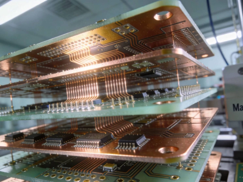
Your stack-up specification tells the manufacturer exactly how to build your board. Ambiguous or incomplete stack-up data causes the most common ordering errors. Don't assume the manufacturer knows what you want just because you're ordering a standard board. State your layer count, copper weights, dielectric materials, and thickness requirements explicitly. When tolerances matter—and they always do for controlled impedance boards—specify those tolerances too.
Differential pair requirements deserve particular attention. If your board includes USB, HDMI, Ethernet, or other differential interfaces, specify the impedance requirements along with acceptable tolerance. The stack-up determines whether those impedance targets are achievable. Give your manufacturer the complete picture—datasheet impedance specifications, connector requirements, and expected manufacturing tolerances—so they can recommend an appropriate stack-up.
Cross-section drawings communicate stack-up visually. A simple table of layer thicknesses may be misinterpreted; a drawing showing the complete layer structure eliminates ambiguity. Many Chinese manufacturers have standard cross-section templates; ask for theirs and fill them in completely. This simple step prevents more errors than almost any other documentation practice.
Drill charts seem straightforward but contain multiple opportunities for error. Via sizes must match the finished plating requirements. Non-plated holes require explicit notation. Blind and Buried Via definitions must be complete enough for the manufacturer to understand the complete drill sequence. Reviewing drill charts carefully before submission catches errors that would otherwise cause manufacturing delays.
Slot and cutout dimensions often create confusion. Is a slot dimension the finished size or the tool size? What's the tolerance on non-standard shapes? These questions need clear answers before manufacturing begins. Provide dimensioned drawings for any slots, cutouts, or complex board shapes—don't rely on the outline layer alone to communicate these requirements.
Duplicate drill sizes deserve verification. Multiple via sizes that appear different may represent the same finished hole diameter after plating. Conversely, vias specified at the same size may need different drill bits depending on whether they're through-holes, blind vias, or buried vias. Cross-check your drill chart against your via requirements to ensure every drill size has a purpose and every requirement has a drill size.
Surface finish selection affects solderability, shelf life, cost, and compatibility with your assembly process. HASL, ENIG, OSP, Immersion Silver, and Immersion Tin each have distinct characteristics. Don't leave surface finish selection to manufacturer preference when your assembly process has specific requirements. If you need lead-free compatibility, specify it explicitly. If your boards will sit in inventory for months before assembly, OSP may not be appropriate.
ENIG specification deserves particular care. Gold thickness affects both cost and durability. Too thin, and the gold may wear through during multiple reflow cycles. Too thick, and the nickel layer becomes brittle. Standard ENIG specifications work for most applications, but your contract manufacturer should know if your process is non-standard. Discuss your assembly requirements with your PCB supplier before specifying ENIG parameters.
Finish transitions between boards in multi-board assemblies need consideration. If you're panelizing assemblies with mixed surface finishes, ensure compatibility across the interface. Some finish combinations create metallurgical problems that affect long-term reliability. When in doubt, consult with your assembly house about finish compatibility in your specific application.
Solder mask seems simple—it's just the green coating, right? The reality involves multiple decisions that affect manufacturing cost and board performance. Mask color options vary by manufacturer and may affect availability and lead time. If you need specific colors for branding or optical requirements, specify them explicitly. Standard green masks are most readily available; specialty colors may add cost or delay.
Mask expansion around pads requires specification. The solder mask opening determines how much pad remains exposed for soldering. Too small, and components may not solder properly. Too large, and the mask doesn't adequately protect traces between pads. Standard mask expansion practices work for most designs, but high-density areas may need custom expansion specifications.
Via tenting and plugging options affect both manufacturing capability and cost. Tented vias cover the via with solder mask; plugged vias fill the via before mask application. Neither option is universally available or appropriate. Specify your via treatment requirements explicitly, and confirm with your manufacturer that they can meet those requirements on your specific board design.
Silkscreen markings identify components, test points, and polarization indicators. Missing or unclear markings cause assembly errors that downstream costs make expensive. If reference designators are critical for your assembly process, ensure they're in your silkscreen layer and visible after assembly. If polarity indicators must persist throughout the board's life, specify materials that won't wear off.
Silkscreen legibility depends on manufacturer capabilities and design practices. Minimum line widths and text heights vary by process. Extremely small text may print unclearly or not at all. Confirm your silkscreen specifications against your manufacturer's minimum capability. If you need small text for space reasons, discuss alternatives like laser marking that can achieve finer detail than traditional silkscreen.
Component values and part numbers on silkscreen add BOM verification value but consume board space. Decide deliberately whether this added verification justifies the area required. Some designs include silkscreen selectively—reference designators without values for some components, full markings for critical parts. Document this policy clearly rather than leaving silkscreen content to default generation.
Panelization determines how your boards ship from the fabrication house and how your assembly house receives them. V-score and tab-route each have distinct characteristics affecting depaneling stress, tool costs, and manufacturing capability. Don't assume your manufacturer will panelize according to your preference unless you specify it.
Panel utilization affects cost directly. High utilization—fitting more boards per panel—reduces per-board cost. But aggressive utilization may constrain routing options and complicate depaneling. Discuss utilization trade-offs with your manufacturer, balancing cost against manufacturability.
Fiducial marks for automated assembly deserve specification. If your assembly house needs fiducials for panel alignment, specify their location and style. Panel fiducials differ from board fiducials; ensure your documentation distinguishes between them. Missing or improperly specified fiducials cause assembly alignment problems that waste the cost savings from optimized panelization.
Controlled impedance specifications require more than a target impedance number. The manufacturer needs to know which nets require impedance control, what the target impedance is, and what tolerance is acceptable. Provide impedance requirements in a table format listing the nets, impedance targets, and tolerances. This documentation prevents the common problem of manufacturers applying controlled impedance selectively to nets that appeared impedance-critical.
Test coupon requirements ensure impedance verification. Controlled impedance boards should include impedance test coupons—specific structures designed to measure the impedance characteristics of the Manufacturing Process. Specify coupon style, location, and whether you need test reports. Without coupons and reports, you have no verification that your impedance requirements were achieved.
Differential pair routing specifications require additional detail. For differential pairs, specify the impedance for each individual conductor and the differential impedance. Some manufacturers can control differential impedance directly; others control single-ended impedance with the differential relationship determined by trace spacing. Understanding these manufacturing realities helps you specify requirements that manufacturers can actually achieve.
Design rules exist in context—minimum trace widths assume specific copper weights, minimum annular rings assume specific plating capabilities. Your design may pass your EDA software checks while containing features your manufacturer cannot produce reliably. Running manufacturer-specific design rule checks before submission catches these incompatibilities before they cause production problems.
Chinese manufacturers publish design rule files for major EDA tools. Download these files and run them against your design before submission. The rule violations flagged aren't necessarily errors—they may represent intentional design choices that you can discuss with your manufacturer. But running these checks ensures you're making informed choices rather than accidental violations of manufacturing capability.
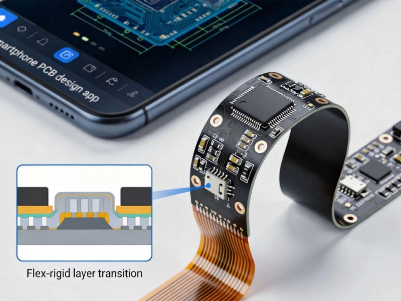
HDI features require specific manufacturer capabilities that vary widely. Blind vias, buried vias, and via-in-pad constructions may require advanced processes that not all manufacturers offer. Before designing with these features, confirm your manufacturer's capability for each feature in your design. Incorporating advanced features into a design destined for a standard capability manufacturer creates fundamental incompatibilities that no documentation can resolve.
A complete documentation package includes Gerber files, drill data, stack-up specifications, drawing packages, and any special requirements. Missing files delay manufacturing while you respond to manufacturer queries. Incomplete specifications create ambiguity that manufacturing fills according to their interpretation rather than your intent. Take the time to prepare complete packages; the investment pays through faster production and fewer errors.
Gerber file review should confirm all expected layers are present and correctly named. Common errors include missing solder mask layers, reversed drill files, and layer naming that doesn't match manufacturer expectations. Use a Gerber viewer to verify your output before submission—these tools reveal problems that EDA software hides.
Revision control prevents confusion when multiple design iterations exist. Include revision numbers and dates in your documentation. When you submit new revisions, ensure the manufacturer acknowledges and implements the updated revision. Tracking revisions through production prevents older revisions from being built when newer versions are intended.
The clearest specifications benefit nothing if communication breaks down during production. Establish direct contact channels with your manufacturer's engineering team. Have escalation paths defined for when problems arise. Respond promptly to manufacturer questions—delayed responses delay production.
First article inspection requests verify that your specifications were understood correctly. When ordering from a new manufacturer or submitting a new design, request first article inspection before committing to full production. This inspection confirms Manufacturing Process outcomes match your expectations, identifying problems while changes remain affordable.
Feedback loops improve future orders. When problems occur, document the root cause and communicate lessons learned to your manufacturer. Similarly, when manufacturers identify specification gaps or unclear requirements, discuss how future documentation can prevent similar issues. This collaborative approach builds relationships that benefit both parties over time.
PCB ordering errors are preventable through disciplined attention to DFM fundamentals and clear specification practices. The ten tips in this guide address the most common sources of ordering problems—from stack-up specification through documentation completeness and communication practices. Applying these principles consistently transforms PCB ordering from a source of anxiety into a reliable engineering process.
The investment in proper DFM practice pays returns immediately through fewer delays and redesigns, and continues paying through improved relationships with capable manufacturers. When your specifications are clear, manufacturers can focus on producing quality boards rather than interpreting ambiguous requirements. This clarity benefits both parties and enables long-term working relationships that compound over multiple orders.
Partner with manufacturers who engage constructively with your DFM practices. The best relationships involve two-way communication—manufacturers who ask clarifying questions rather than assuming, customers who appreciate questions as quality assurance rather than delays. Building these relationships takes time but creates manufacturing partnerships that support your engineering success.

Finding the Right China Flexible PCB Manufacturer for Wearable TechJune/12/2026

Top 5 Applications of HDI PCBs in Modern ElectronicsMay/13/2026

Behind the Scenes: A Tour of Our State-of-the-Art PCB Factory in ChinaMay/19/2026

The Future of PCB Manufacturing in China: Trends for 2026 and BeyondMay/19/2026
The Ultimate Guide to HDI PCB Technology You Need to KnowJune/02/2026
What is Rigid-Flex PCB? Complete Guide from China ManufacturerMay/18/2026
The Complete Guide to SMT PCB Assembly in ChinaJune/17/2026

Detailed Explanation of the Types, Materials, and Applications of Flexible Circuit Boards 101June/04/2026