Open Nav

Multilayer PCBs represent the advanced standard in modern Electronics Manufacturing, enabling complex devices we use daily. From smartphones to servers, these sophisticated circuit boards pack exceptional functionality into compact spaces. As a China PCB Manufacturer with 15+ years producing 120M+ multilayer boards annually, we're sharing our comprehensive expertise to help you understand this essential technology.
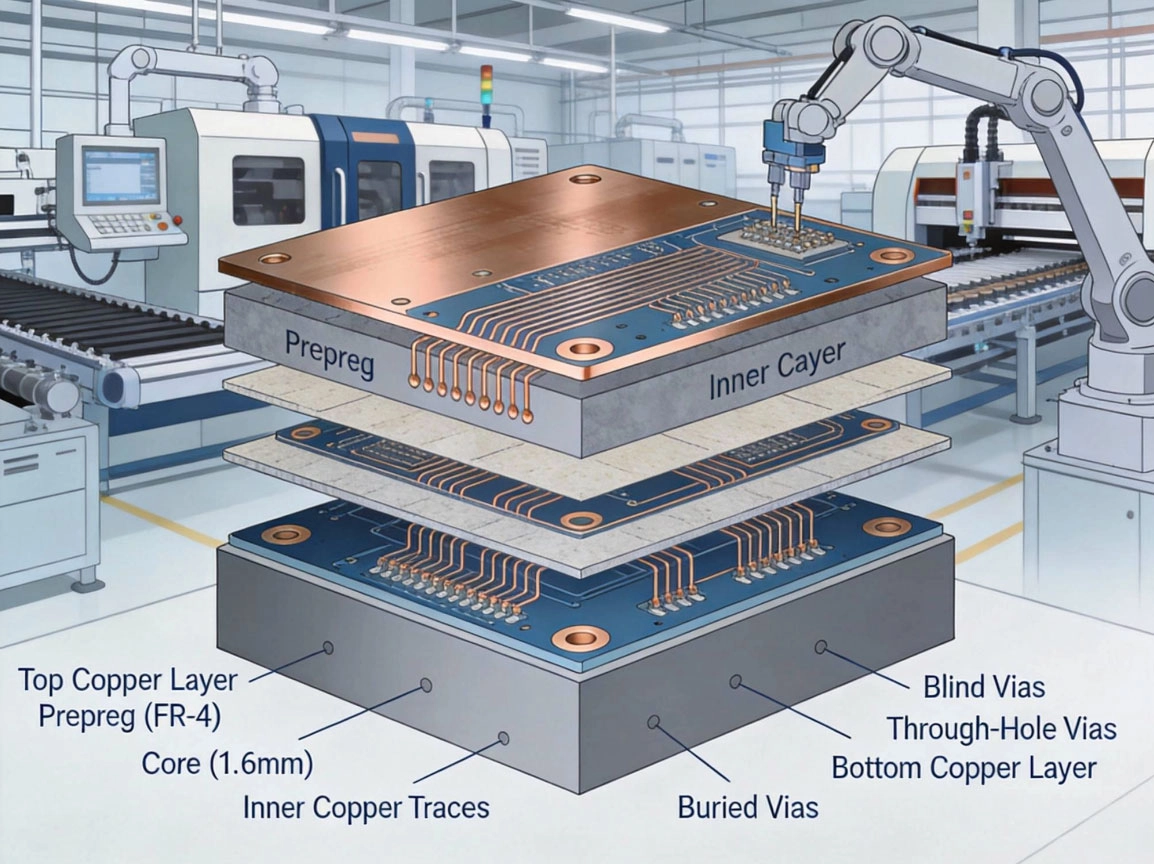
Multilayer printed circuit boards consist of three or more conductive copper layers laminated with insulating prepreg and bonded under heat and pressure. Unlike single or double-sided boards with conductive layers only on outer surfaces, multilayer PCBs route circuits across multiple internal layers, dramatically increasing circuit density within the same footprint.
The technology emerged in the 1960s for military aerospace applications and has since become mainstream across consumer electronics, automotive, communications, and industrial sectors. China now produces over 60% of global multilayer PCBs, offering unmatched scale, cost efficiency, and manufacturing capability.
Every Multilayer Pcb shares core characteristics:- 3+ conductive copper layers (industry standard 4-32 layers)- Insulating prepreg and core materials between layers- Plated vias connecting layers electrically- Symmetric Stackup Design for stabilityMinimum layer count is 4, though 3-layer designs exist for specific cost optimization. Consumer electronics typically use 4-8 layers, while high-performance applications like servers and aerospace systems use 12-32+ layers.
Multilayer PCBs integrate five fundamental elements:
Core Layers form the central foundation—rigid insulating substrates (typically FR-4) pre-clad with Copper Foil. Core thickness ranges from 0.1mm to 2.0mm with copper weights from 18μm to 70μm.
Prepreg Layers are fiberglass cloth impregnated with partially cured epoxy resin that fully cures during lamination, bonding adjacent layers while providing electrical insulation between conductive layers. Thickness is precisely controlled from 0.05mm to 0.2mm for impedance characteristics.
Copper Layers form circuit traces carrying signals, power, and ground. Outer layers have component mounting pads while inner layers serve routing, power distribution, and ground planes. Standard copper thicknesses: 18μm (1/2 oz), 35μm (1 oz), 70μm (2 oz).
Via Structures enable electrical connections between layers:- Through-hole vias connect all layers- Blind Vias connect outer to inner layers- Buried Vias connect only internal layers- Microvias (laser-drilled under 0.15mm) for high-density designs
Via technology enables efficient complex circuit routing across multiple layers.Solder Mask and Surface Finish protect outer layers with mask coating preventing shorts, followed by surface finish (Enig, Immersion Silver, Osp, Hasl) protecting pads and ensuring solderability.
4-Layer PCBs (most common configuration):- Layer 1 (Top): Signal + components- Layer 2: Ground plane- Layer 3: Power plane- Layer 4 (Bottom): Secondary signal + componentsApplications: Smart homes, basic IoT, industrial controls, automotive body electronics. Thickness: 0.8-1.6mm.
6-Layer PCBs add two signal layers in Signal-Ground-Signal-Signal-Power-Signal configuration. Applications: Smartphones, tablets, automotive infotainment, medical devices. Thickness: 1.2-2.0mm.
8-Layer PCBs provide higher routing density with dedicated high-speed, analog, multiple power domain, and ground plane layers. Applications: Laptops, network routers, automotive ADAS, medical imaging. Thickness: 1.6-2.4mm.
10-20 Layer PCBs for performance-critical applications with multiple specialized layers. Applications: Servers, 5G infrastructure, aerospace, medical imaging. Thickness: 2.0-3.2mm.
20+ Layer High-Density PCBs incorporate HDI Microvia Technology, advanced materials, and strict impedance control. Applications: Supercomputers, network switches, satellites, military electronics. Thickness: 3.0-6.0mm.
Multilayer PCBs deliver compelling benefits:
Dramatically Higher Circuit Density - Additional routing layers enable 2-3x the functionality of double-sided boards in the same footprint.
Superior Electrical Performance - Dedicated power and ground planes provide stable power distribution, Controlled Impedance, better EMI shielding, and clean signal return paths minimizing crosstalk.
Improved Reliability - Eliminates thousands of solder connections between multiple boards, reducing potential failure points. Laminated structure provides superior mechanical stability and vibration resistance.
Overall Cost Reduction - Eliminates connectors, cables, and assembly labor. Reduces product size and weight for lower packaging and shipping costs. Improves reliability reducing field failure costs.
Design Flexibility - Separates analog and digital sections, implements multiple isolated power domains, optimizes layer stackups for impedance, creates specialized shielding for noise-sensitive circuits.
China produces 60%+ of global multilayer PCBs due to:
Manufacturing Scale - Billions invested in production capacity, facilities producing millions monthly, economies of scale driving costs down.
Advanced Technology - Leading capabilities: 40+ layers, HDI microvias down to 0.075mm, ±5% impedance control, high-Tg FR-4, low-Dk laminates, high-frequency materials, rigid-flex and metal core capabilities.
Cost Competitiveness - 30-50% less than Western production without quality sacrifice. Advantages: local material supply chains, optimized high-volume processes, competitive skilled labor, lower operating expenses.
Quality Systems - Comprehensive certifications: Iso 9001, Iatf 16949 (automotive), Iso 13485 (medical), AS9100 (aerospace), UL safety certification. Defect rates below 200 DPMO for volume production.
Supply Chain Ecosystem - Complete Electronics Supply Chain enabling integration between Pcb Manufacturing, component sourcing, assembly—reducing lead times, simplifying logistics, lowering overall product cost.
Consumer Electronics: Smartphones, laptops, tablets, gaming consoles, smart watches, appliances
Automotive: ECUs, infotainment, ADAS sensors, EV battery management
Communications: 5G base stations, routers, switches, servers, data center equipment, mobile devices
Industrial: PLCs, automation, power supplies, test instruments
Medical: Patient monitors, diagnostics, implants, imaging
Aerospace/Defense: Avionics, satellites, communications, guidance systems
Every electronic device today incorporates at least one Multilayer Pcb.Use symmetric stackups - Balanced layer counts and copper distribution prevent warping during lamination and operation
Include dedicated ground planes - Essential for noise control and signal return paths
Separate analog and digital sections - Isolate sensitive analog from noisy digital to prevent interference
Control trace impedance - Work with manufacturer early to define stackup and trace geometries
Follow manufacturer design rules - Adhere to Minimum Trace Width, spacing, via size for optimal yield
Request Dfm review - Get Design For Manufacturability review from manufacturer before finalizing design
Cost depends on layer count, complexity, volume. Generally: 4-layer 1.5-2x more than double-sided, 6-layer 2-3x more, 8-layer 2.5-4x more. However, multilayer often reduces total system cost by eliminating connectors/cables/assembly steps.
Most common standard: 1.6mm (0.0625") for 4-8 layers. Thinner: 0.8-1.2mm for space-constrained. Thicker: 2.0-3.2mm for higher layer counts/rigidity/higher current.
Standard volume production: minimum trace/space 0.1mm (4mil), via diameter 0.2mm (8mil), annular ring 0.075mm (3mil). Advanced HDI extends to 0.05mm (2mil) trace/space and 0.075mm (3mil) microvias.
Standard lead times: 4-6 layer prototypes 3-5 days, 8-12 layer prototypes 5-7 days, 12+ layer prototypes 7-10 days. Volume production: 10-15 days for most configurations. Expedited services reduce lead times 30-50% for additional cost.
Standard FR-4 most common. High-Tg FR-4 (≥170°C) for higher thermal stability. Specialized: low-Dk laminates for high-frequency, polyimide for high-temperature, metal cores for high-power Thermal Dissipation.
Multilayer PCBs enable the digital revolution, making increasingly compact, powerful, affordable electronics possible. As designs grow in complexity while shrinking in size, multilayer PCBs remain the foundational technology for electronics.
China's global leadership in multilayer Pcb Manufacturing provides product developers with advanced capabilities at competitive prices. From simple 4-layer designs to complex 32-layer high-speed assemblies, experienced China PCB manufacturers like ours support projects with free Dfm reviews, quick prototyping, volume production, and comprehensive engineering support.
Ready to start your multilayer PCB project? Upload design files today for free quotation and Dfm Review. We provide quick prototyping, volume production, and engineering support ensuring project success.
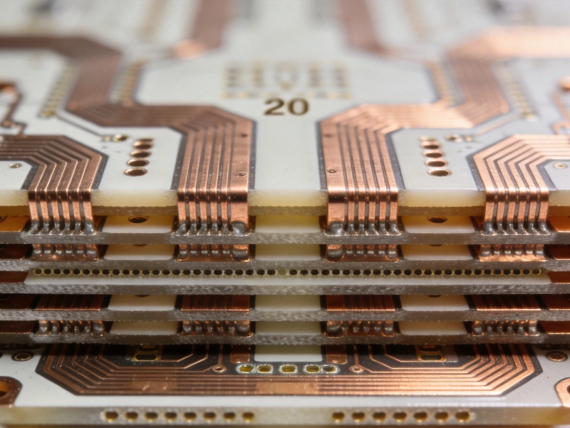
How to Design High-Layer Count PCBs (20+ Layers) for Complex ElectronicsSeptember/08/2026
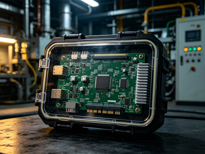
Durability Requirements for Industrial IoT PCBs: Ensuring Reliability in Harsh EnvironmentsSeptember/03/2026
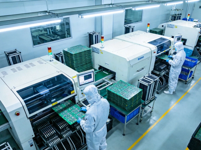
Behind the Scenes: A Tour of Our State-of-the-Art PCB Factory in ChinaMay/19/2026
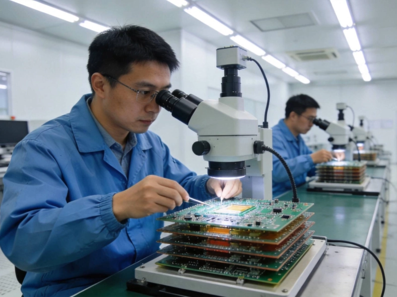
How We Ensure Quality Control in Multilayer PCB LaminationAugust/08/2026
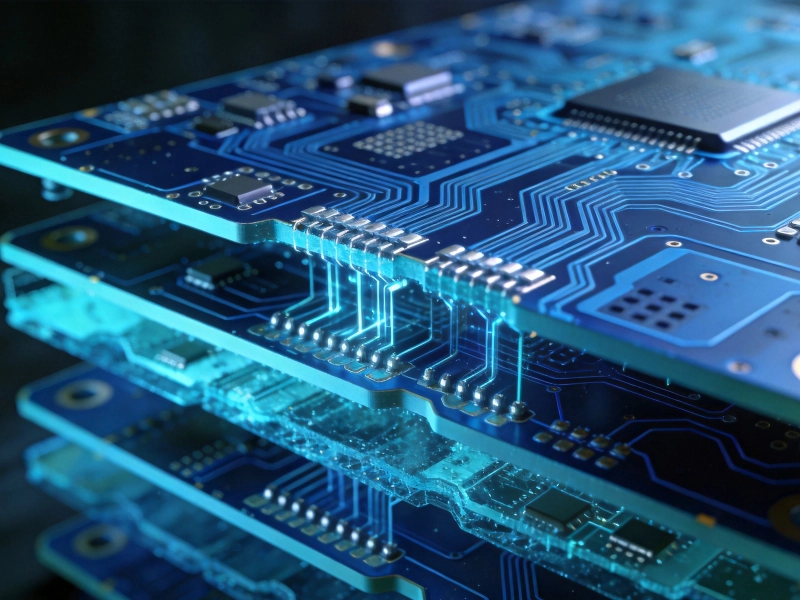
Understanding HDI PCB Stack-ups: Best Practices for High-Density DesignsJuly/18/2026
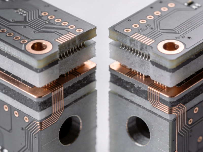
Microvias vs. Through-Holes: Choosing the Right Tech for Your Multilayer BoardAugust/06/2026
Implantable Medical Devices: Precision and Reliability in PCB ManufacturingSeptember/24/2026
Case Study: Solving a Complex Thermal Issue with a Metal Core PCBOctober/12/2026