Open Nav

Designing High-density Interconnect (HDI) printed circuit boards demands careful attention to trace width specifications. Unlike conventional PCB designs, HDI boards push the boundaries of Miniaturization, requiring engineers to understand exactly what minimum trace width they can achieve without compromising manufacturing yield or board reliability.
The short answer: most Hdi Pcb manufacturers can produce trace widths as narrow as 50-75 microns (2-3 mils) in production, with some advanced facilities handling traces down to 30-40 microns for ultra-fine-pitch applications. But here's the thing — that minimum isn't a fixed number. It varies based on your board's layer count, material selection, and the specific fabrication partner you're working with.
In this guide, I'll walk you through everything you need to know about Hdi Pcb trace width constraints, from basic fundamentals to practical design recommendations that won't leave you with manufacturing headaches.

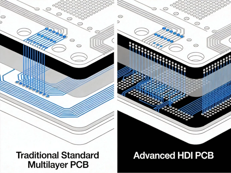
Before diving into trace width specifics, let's clarify what makes HDI boards different from their standard counterparts. HDI PCBs feature higher wiring density per unit area, typically achieved through Microvias with diameters under 150 microns, finer trace geometries, and often incorporates blind and Buried Via structures.
These characteristics enable significant size reduction — you might see 40-60% smaller packages compared to through-hole designs. But achieving that density requires tighter design rules, and trace width sits right at the center of those constraints.
The move from Through-hole Technology to HDI isn't just about making things smaller. It's about enabling functionality that wouldn't be possible at larger geometries — think smartphones, wearable devices, and medical implants where space is at an absolute premium.
Here's a practical breakdown of what you can expect:
For boards with 1-2 Sequential Lamination cycles, minimum trace widths typically land in the 75-100 micron range (approximately 3-4 mils). This represents a sweet spot where most manufacturers offer consistent yields and competitive pricing. At this level, you're still within the comfort zone for most fabrication houses, even those without cutting-edge equipment.
When your design requires three or more build-up layers — common in complex smartphones and advanced computing hardware — you can push down to 50-75 microns (2-3 mils). This tier requires more sophisticated manufacturing capabilities and often commands a premium, but it unlocks significant area savings.
The bleeding edge of Pcb Technology brings substrate-like printed circuit boards (SLPs) with trace widths reaching 30-40 microns (1.2-1.5 mils). Samsung pioneered this category with their "semi-additive process" (SAP) designs, and it's becoming increasingly common in flagship mobile devices. Not every manufacturer can produce these geometries reliably, so your fab selection becomes critical.
Several variables influence what you can actually achieve. Ignoring these factors when setting your design rules is a surefire way to get quotes that don't match reality or, worse, boards that come back with Manufacturing Defects.
Starting copper weight sets your baseline. Standard 1 oz copper (35 microns) after etching produces different final dimensions than lighter or heavier options. Add to that the copper plating that builds up on sidewalls during through-hole plating — this can consume 15-25 microns of your trace width budget, which matters when you're designing at 50-micron scales.
If you need ultra-fine traces, consider starting with lower copper weights (½ oz or ¼ oz) and using plate-up techniques to achieve your target thickness selectively.
The dielectric material affects both trace integrity and minimum achievable width. Low-flow prepregs used in Sequential Lamination can cause trace flow-out, effectively widening traces beyond your design intent. High-performance materials like Rogers or Panasonic Megtron grades offer better dimensional stability but at significantly higher cost.
Material selection also impacts impedance control, which often dictates trace width more strictly than pure manufacturing capability. If you're designing 90-ohm USB traces or 100-ohm differential pairs, your width tolerances might be tighter than pure manufacturing limits.
More layers generally means more constraints. Each lamination cycle introduces dimensional variation, and designs with blind and Buried Vias often face additional design rules that restrict trace routing near via structures. A 10-layer HDI board will have different minimum trace requirements than a simple 4-layer build-up design.
This might be the most variable factor. I've seen quotes range from 65 microns to 100 microns for seemingly identical specifications, simply because one fab has newer equipment or specializes in high-density work. When trace width is critical to your product, visiting potential manufacturing partners or requesting capability reviews pays dividends.
Getting your HDI traces right isn't just about hitting the minimum — it's about designing traces that your manufacturer can produce consistently, at scale, with acceptable yields. Here's what I've learned works well in practice.
Never design to the absolute minimum capability of your target fab. Add at least 20-25% margin above the published minimum. If your fab quotes 75 microns as their minimum, design for 90-100 microns unless space constraints genuinely require pushing limits. This margin accounts for process variation across panels, lot-to-lot differences, and the inevitable realities of production manufacturing.
Minimum trace width means little without considering minimum spacing. Many manufacturing issues arise from spacing violations rather than width problems. HDI designs typically require spacing equal to or greater than trace width, and this relationship becomes more critical at finer geometries. Design rules that treat width and spacing as independent variables often lead to surprises on the manufacturing floor.
For traces carrying significant current, you'll need wider traces than pure geometry would suggest. HDI boards aren't immune to current-carrying requirements, and designing 50-micron traces for a power rail that needs 500mA capability is a recipe for reliability failures. Use IPC current capacity calculators as starting points, but validate with thermal simulation for critical nets.
As traces get narrower, they become more susceptible to manufacturing variations that affect impedance. If you're routing high-speed signals (anything above 1 GHz effective data rate), consider whether your fab can hold the impedance tolerances your design requires at the trace widths you're specifying. +/- 10% impedance control at 50-micron widths is challenging; +/- 5% is even more so.
Having reviewed dozens of HDI designs that ran into manufacturing issues, certain patterns recur. Here's how to avoid them.
One of the most common errors is assuming that design software minimums equal manufacturing minimums. Your EDA tool might show 25-micron traces as perfectly valid, but that doesn't mean any fab can produce them. Always, always validate against your specific manufacturer's capabilities before finalizing your design rules.
Another frequent issue involves mixing trace width specifications across different net classes without clear documentation. A design might have 75-micron signals, 100-micron power traces, and 150-micron RF structures all in the same stack-up. When manufacturing documentation isn't explicit about these differences, you get confusion and potentially incorrectly produced boards.
Finally, watch out for thermal stress issues in ultra-fine trace designs. Traces below 50 microns can experience electromigration or delamination under high-current or thermal cycling conditions. If your product will see demanding environments, prototype testing becomes non-negotiable.
The relationship between designer and manufacturer makes or breaks HDI projects. Here's how to set yourself up for success.
Start with a design review request before finalizing your artwork. Most serious HDI manufacturers offer this service free or at low cost, and they'll flag rule violations specific to their process capabilities. This single step can save weeks of debug time and thousands in re-tooling costs.
Be explicit about your priority: is space saving paramount, or is first-pass yield more important? These goals sometimes align, but they can also conflict. A manufacturer told to prioritize yield might choose more conservative design rules than one optimizing for minimum feature size.
Request cross-sectional analysis of sample boards before committing to production. Looking at actual trace profiles under a microscope reveals a lot about process capability and what your design will actually look like when manufactured. This is particularly important if you're pushing toward the fine end of achievable geometries.
Let's address the elephant in the room: finer traces cost more. There's no way around this reality. Ultra-fine line HDI requires specialized equipment (laser direct imaging, advanced etching systems), more rigorous process controls, and typically lower throughput during manufacturing.
That said, the cost premium often makes economic sense when you factor in what you're getting. If going from 100-micron to 60-micron traces allows a 30% reduction in board area, you might save more on enclosure costs, connectors, and assembly than you spend on PCB Fabrication. Run the full system Cost Analysis before dismissing fine-line designs based on unit PCB price alone.
Volume matters significantly. A 10,000-unit annual build can support more advanced HDI capabilities than a 500-unit medical device where NRE costs dominate. Understand how your volume profile affects both what's available and what's economically rational.
The industry continues pushing toward finer geometries. SAP and modified semi-additive process (mSAP) technologies are becoming more accessible, enabling traces below 30 microns. While not mainstream today, these capabilities will increasingly become standard options over the next few years.
Embedded passives and active components are also reducing the pressure on trace density in some applications. By integrating resistors and capacitors directly into the board structure, designers can reclaim routing area that would otherwise require fine-trace fanout.
Panel-level packaging represents another frontier, treating the PCB more like a semiconductor substrate. This approach, being developed by companies like AT&S and Unimicron, takes fine-line capability as a given rather than a challenge.
Minimum trace width for HDI PCBs isn't a single number — it's a range that depends on your specific requirements and manufacturing partner. Standard HDI typically supports 75-100 micron traces, advanced HDI enables 50-75 microns, and ultra-fine designs can reach 30-40 microns with specialized processes.
Design to your manufacturer's actual capabilities, not theoretical software minimums. Add margin above published minimums, consider spacing rules equally, and validate through cross-section analysis before high-volume production. Cost premiums for fine traces often make sense when evaluated at the system level rather than the PCB alone.
Start conversations with potential manufacturers early, leverage their design review services, and always prototype at production-intent fabs before committing to volume. These practices won't just improve your HDI designs — they'll transform how you approach high-density development altogether.
Most established HDI fabricators can reliably produce 75-micron (3-mil) traces in production volumes. Advanced manufacturers with newer equipment commonly handle 50-65 microns, while only a select few can consistently produce traces below 40 microns using advanced SAP processes.
Yes, most HDI designs incorporate multiple trace width specifications for different net classes. Signal traces might be 60 microns, power buses 120 microns, and RF structures 200 microns or wider. Document these specifications clearly for your manufacturer to ensure correct processing.
Finer trace widths generally increase PCB cost due to more precise processing requirements, lower throughput, and higher defect rates. However, the premium is often justified when the space savings reduce overall system cost through smaller enclosures, fewer layers, or simplified assembly.
Cross-sectional analysis provides definitive verification of trace width and profile. Automated Optical Inspection (Aoi) can identify defects but typically can't measure absolute dimensions precisely. For critical applications, impedance testing and thermal cycling combined with cross-sections provide comprehensive validation.
Narrower traces can actually benefit Signal Integrity by enabling shorter routes and reducing stubs. However, they also present challenges for impedance control due to tighter manufacturing tolerances and increased sensitivity to dielectric thickness variation. Balance density needs against Signal Integrity requirements for your specific application.
If you're designing your first HDI product, consider starting with more conservative trace widths and moving to finer geometries only when you've validated your design approach and manufacturing relationship. It's better to have a slightly larger board that works than an aggressively compact design that doesn't yield consistently.
Ready to start your HDI design journey? Focus on finding a manufacturing partner whose capabilities align with your product requirements, and don't underestimate the value of early design reviews. The best HDI designs aren't those that push every parameter to its theoretical limit — they're the ones that achieve the right balance between density, reliability, and producibility.
Understanding HDI PCB Technology: A Comprehensive Guide for BeginnersMay/13/2026
HDI PCB vs Standard PCB: Key Differences ExplainedMay/13/2026
The Ultimate Guide to HDI PCB Technology You Need to KnowJune/02/2026
Why Choose a China HDI PCB Manufacturer for Your Project?May/13/2026
What is HDI PCB? A Complete Guide from China HDI PCB ManufacturerMay/13/2026

How to Choose the Best China HDI PCB Manufacturer in 2026June/08/2026

HDI PCB Manufacturing Process: Step-by-Step ExplanationMay/13/2026

Top 5 Applications of HDI PCBs in Modern ElectronicsMay/13/2026