
Every engineering team faces the same pressure: deliver reliable products while keeping expenses under control. Pcb Manufacturing often represents a significant portion of electronics production budgets, and cost overruns here can derail entire projects. The good news is that reducing PCB costs doesn't mean accepting lower quality or higher failure rates.
This guide walks through practical approaches to lower your Pcb Manufacturing expenses without compromising the reliability your products demand. From design-stage decisions to supplier relationships, you'll find actionable strategies that work in real production environments.
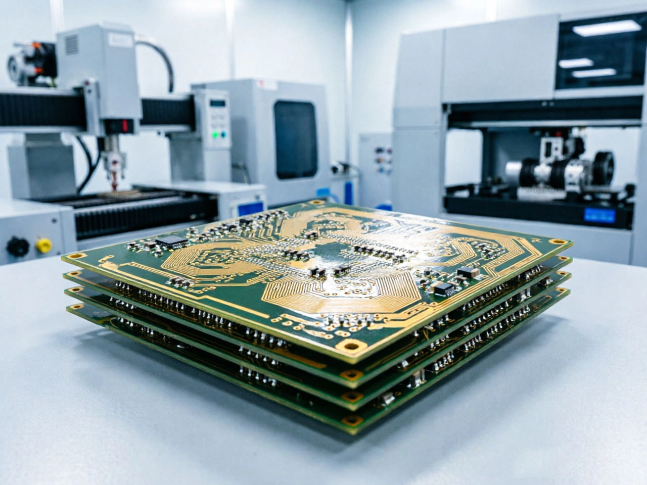
Before you can reduce costs, you need to understand where your money actually goes. PCB pricing typically breaks down into several categories:
When engineering teams overlook these factors during design, they often pay much higher prices than necessary. Most cost-saving opportunities exist in the design phase, before manufacturing even begins.
The decisions your engineering team makes on the schematic and layout directly determine manufacturing expense. Optimizing designs for producibility is the single most effective way to reduce costs.
Multi-layer PCBs scale dramatically in cost with each additional layer. A 4-layer board might cost 40-60% less than an equivalent 6-Layer Design. Before committing to a specific stackup, challenge your routing requirements honestly.
Can you achieve your Signal Integrity goals with fewer layers? Strategic placement of ground planes and careful routing often eliminates the need for additional layers. Reserve higher layer counts for designs where the electrical requirements genuinely demand them, such as high-speed interfaces or complex mixed-signal applications.
Manufacturers produce PCBs in standard panel sizes—typically 18x24 inches or 21x24 inches in Asia. Boards that fit efficiently into these panels yield more boards per panel, directly reducing your per-unit cost.
Work with your manufacturer to determine optimal board dimensions for your volume. Sometimes slight adjustments to board size—like increasing width by a few millimeters—can double the number of units per panel. This optimization becomes especially valuable at higher production volumes.
Blind Vias, Buried Vias, and Microvias add substantial processing steps and reduce manufacturing yields. Each additional process step introduces potential failure points and increases labor time.
Evaluate whether alternative designs can achieve your goals without these premium features. For many applications, through-hole vias with appropriate annular rings provide adequate performance at significantly lower cost. Reserve advanced interconnect technologies for designs where conventional approaches genuinely cannot meet specifications.
Drilling represents a major cost center in PCB manufacturing. The number of different drill sizes, aspect ratios, and via types all impact processing time and tooling wear.
Consolidate drill sizes where possible. If your design uses six different drill diameters, consider whether you can standardize on three or four. Also be mindful of via aspect ratio—deep small-diameter holes require specialized equipment and extended processing time.
Many companies treat Dfm review as a final checkpoint before production. Forward-thinking teams integrate Dfm considerations throughout the design process.
Collaborate with your manufacturer early in the design cycle. Most established PCB suppliers offer design reviews that identify potential manufacturability issues before tooling begins. Catching problems at this stage costs only engineering time. Discovering them after production starts can mean scrapped boards and delayed schedules.
Key DFM considerations include:
Your choice of PCB manufacturer significantly impacts both cost and quality. Building the right supplier relationship requires looking beyond unit pricing.
A manufacturer offering 15% lower per-unit pricing might deliver worse overall economics if their quality issues require additional inspection steps, generate higher scrap rates, or cause field failures. Consider the complete cost picture:
PCB manufacturing carries substantial setup costs for tooling, artwork preparation, and process setup. Manufacturers naturally price these amortized costs across expected volume. Designs with predictable, higher volumes receive better economics.
If your product roadmap allows, consider consolidating multiple board designs with similar specifications. A manufacturer producing 10,000 units annually across three board types may offer better pricing than three separate orders of 3,333 units each.
Transactional supplier relationships—constantly switching manufacturers for the lowest quote—rarely achieve the best outcomes. Each transition introduces learning curve costs, potential quality variations, and communication friction.
Invest in relationships with one or two key suppliers. Share your product roadmap. Give them visibility into your volume expectations. Long-term partners invest in understanding your requirements and often proactively suggest cost-reduction ideas.
PCB substrate materials range widely in performance and price. Selecting the right material for your application—not the most expensive option—yields substantial savings.
High-performance laminates like Rogers or Panasonic materials offer superior electrical properties for RF and high-speed digital applications. But these materials carry 3-10x the cost of standard FR-4 materials.
For many designs, especially those operating below 1 GHz or without critical impedance requirements, standard FR-4 grades provide entirely adequate performance. Don't overspecify materials based on theoretical performance margins your application never exercises.
Heavier copper weights increase current handling capacity but also raise material costs and affect impedance calculations. Evaluate your actual current requirements honestly and specify copper weights accordingly.
For many power applications, using 2 oz copper on outer layers only—rather than heavy copper throughout the stackup—achieves adequate current handling while controlling costs.
How your boards assemble onto manufacturing panels directly affects production efficiency and cost.
Manufacturers price boards partly based on panel utilization. More boards per panel means better efficiency and lower per-board cost. Work with your supplier to design arrays that maximize panel usage.
Standard panel sizes and common array configurations exist for good reason—they represent proven, efficient production setups. While unique panel designs sometimes serve specific assembly needs, they often carry cost premiums.
Mouse bite tabs connecting boards to panel rails must balance reliable connection during assembly with clean separation after depanelization. Improperly designed tabs can cause board damage or require extra labor to remove.
Follow manufacturer guidelines for tab width, spacing, and routing. V-score depths, mouse bite sizes, and tab placement all affect both manufacturing yield and post-assembly handling.
Every PCB requires some level of testing, but testing scope should match actual quality requirements rather than following arbitrary standards.
100% electrical testing of every net might be essential for medical devices or safety-critical automotive applications. For many consumer electronics, statistical sampling during batch testing provides adequate Quality Assurance at lower cost.
Discuss your actual reliability requirements with your manufacturer. They can often suggest testing approaches that match your risk profile and application requirements.
Test points, probe access points, and clearages for flying probe testers reduce test time and improve coverage. Adding 2-3 mils of clearance around critical test points costs nothing in board space but can significantly reduce test setup time.
Include test coupons in panel artwork for statistical process control. These allow manufacturers to verify process quality without testing every production board.
Reducing PCB manufacturing costs while maintaining quality requires attention across the entire product lifecycle. The most significant opportunities exist in design decisions—layer count, board dimensions, material selection, and technology choices all compound throughout production.
Build relationships with capable manufacturers who understand your application requirements. Engage them early in the design process. Let them contribute their expertise to optimize designs for efficient production.
The goal isn't finding the cheapest possible manufacturing option—it's eliminating unnecessary costs while maintaining the quality your products and customers require. Strategic investment in Design Optimization and supplier relationships typically delivers better results than pursuing lowest-unit-price quotations.
Design Optimization typically offers the highest return on investment. Right-sizing layer count, standardizing board dimensions, and minimizing special processes can reduce costs by 30-50% compared to unoptimized designs. These decisions made during design lock in cost structure for the entire production run.
Not necessarily. Cost Reduction strategies focused on eliminating unnecessary complexity—like reducing excess design margins or optimizing panel utilization—do not affect board reliability. However, cutting costs by accepting substandard materials, reducing inspection, or choosing unreliable manufacturers can definitely impact quality.
Reducing from 6 layers to 4 layers typically saves 40-60% on that portion of the board cost. For a multi-layer board, this might translate to 20-30% overall Cost Reduction. The actual savings depend on specific designs and quantities.
Not always. The lowest quote may not reflect Total Cost Of Ownership. Consider first-pass yield rates, defect rates, delivery reliability, and engineering support quality. A manufacturer with 2% higher pricing but 99.5% yield may offer better economics than a cheaper competitor with 95% yield.
High-performance substrates become necessary for applications with specific electrical requirements: RF circuits above 1 GHz, high-speed digital interfaces with critical impedance tolerances, or boards with significant loss concerns. For typical digital logic and lower-frequency analog circuits, standard FR-4 materials usually perform adequately.
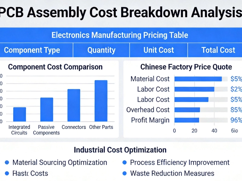
PCB Assembly Price China: A Complete Cost Guide for 2024May/18/2026
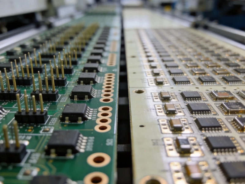
Thru-Hole vs. SMT: Choosing the Right Assembly Technology for Your PCBJuly/10/2026

Understanding PCB Assembly Prices in China: What Factors Influence Cost?June/10/2026
The Complete Step-by-Step Process ExplainedJune/05/2026
Cost-Benefit Analysis of Rigid-Flex PCBs vs. Traditional Cable AssembliesSeptember/14/2026
How Automated Optical Inspection (AOI) Ensures SMT QualityAugust/15/2026
What is a Multilayer PCB? A Comprehensive Guide for EngineersJuly/02/2026

BGA Assembly Challenges: X-Ray Inspection and Voiding IssuesSeptember/17/2026