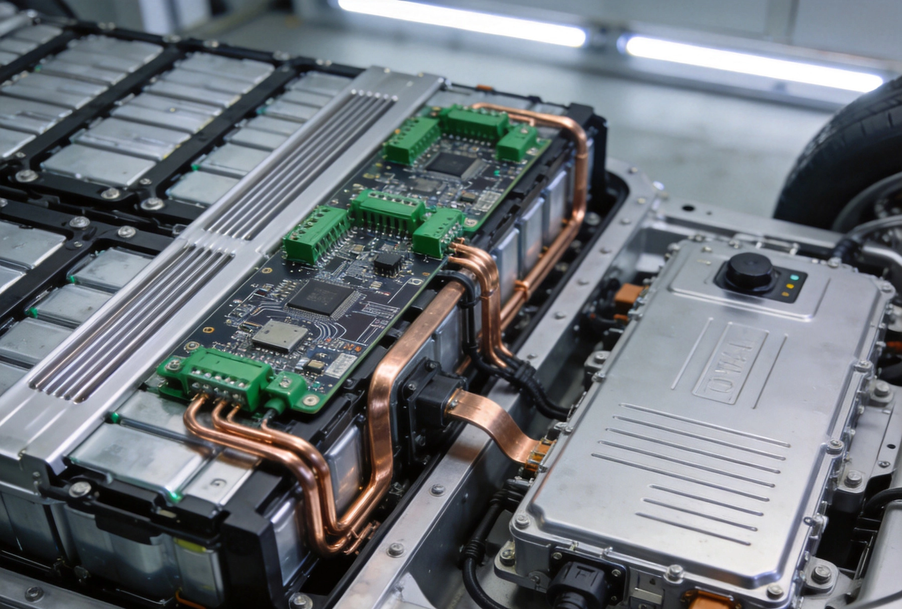
Electric vehicles represent one of the most demanding applications for power electronics, and nowhere is this more apparent than in the Battery Management System (BMS) that monitors, balances, and protects the massive battery packs delivering hundreds of kilowatts to vehicle drivetrains. The BMS must accurately sense cell voltages and temperatures across hundreds of individual cells, execute complex algorithms to estimate state-of-charge and state-of-health, communicate with vehicle control systems, and crucially, handle fault conditions that could otherwise result in thermal runaway. Every one of these functions depends on Pcb Technology that can reliably manage heat, carry high currents, and operate dependably for the vehicle's lifetime.
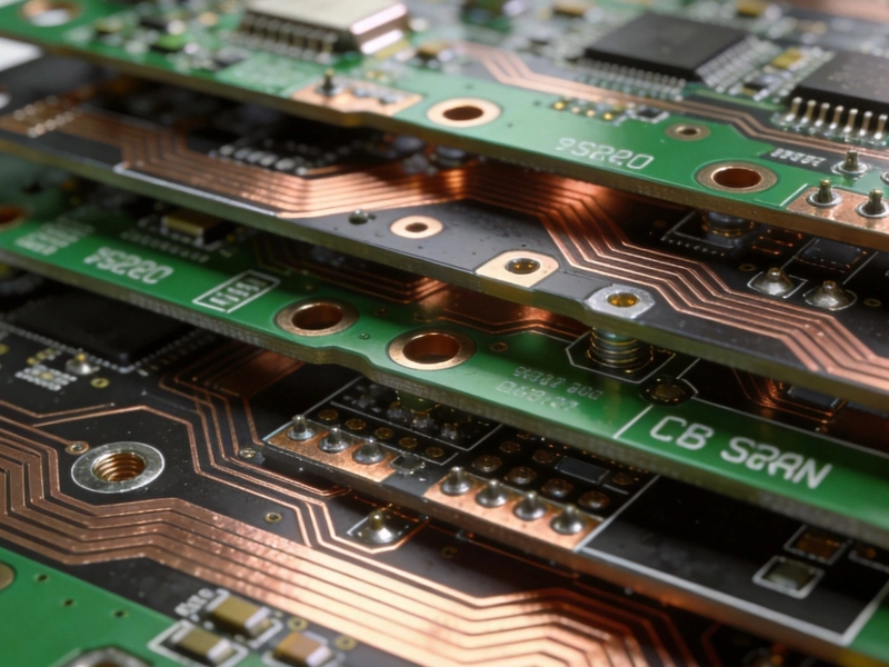
Heavy copper PCBs have emerged as the enabling technology for modern EV BMS architectures. These boards, with copper weights ranging from 2oz to 6oz or heavier, provide the current-carrying capacity, thermal performance, and reliability that battery management applications demand. Understanding how heavy copper technology integrates into BMS design reveals why this seemingly specialized PCB approach has become essential for the electric vehicle industry.
A Battery Management System in an electric vehicle performs multiple critical functions that keep the battery pack operating safely and efficiently. Cell monitoring involves measuring individual cell voltages with millivolt accuracy and cell temperatures at multiple points throughout the pack. This sensing data feeds algorithms that estimate remaining range, optimize charge and discharge profiles, and detect abnormal conditions before they escalate into safety hazards.
Charge balancing compensates for variations between cells that develop over the pack's lifetime. Active balancing circuits transfer energy from higher-charged cells to lower-charged cells, while passive balancing dissipates excess energy as heat through resistors. Both approaches require Pcb Technology that can handle localized heating without compromising measurement accuracy or long-term reliability. The balancing circuits often carry amps of current continuously during charging, creating thermal demands that standard PCB constructions cannot sustainably address.
Contactors and precharge circuits manage the connection between battery pack and vehicle high-voltage bus. These circuits must handle hundreds of amps during vehicle acceleration and charging, switching reliably for the thousands of cycles that constitute a vehicle lifetime. The PCB traces carrying this current must maintain low resistance despite thermal cycling and aging, with resistance increases that could cause excessive heating or voltage drop problems monitored as part of the vehicle's diagnostics.
Electric vehicle battery packs operate in environments that stress conventional electronics. Ambient temperatures can swing from well below freezing in winter climates to elevated temperatures in hot climates with limited parking shade. Vehicle vibration from road surface, drivetrain, and thermal expansion cycles creates mechanical stress on solder joints and component terminations. The battery pack itself generates heat during high-power charging and discharging, adding to the thermal burden that electronics must survive.
The BMS must continue functioning throughout these conditions, maintaining measurement accuracy even as component temperatures vary by 40°C or more during normal operation. Heavy copper PCBs contribute to thermal stability by spreading heat laterally across the board plane, reducing temperature gradients that would otherwise cause measurement drift or component stress. The copper mass absorbs thermal transients, moderating peak temperatures during high-current events before cooling systems catch up.
Balancing circuits in high-capacity EV battery packs routinely carry 1A to 5A per channel, with dozens of channels operating simultaneously. For a 100kWh pack with 400V architecture, the balancing circuits might dissipate 50W to 200W during intensive equalization. At these power levels, trace width calculations based on standard 1oz copper produce results measured in centimeters—impractical for dense automotive layouts. 2oz or 3oz copper reduces required trace widths proportionally, enabling routing that fits within the physical constraints of the battery enclosure.
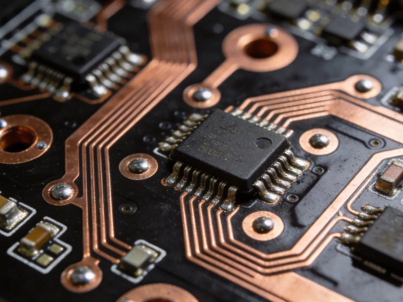
Main current paths carrying charge and discharge current face even more demanding requirements. The sense resistors that measure pack current for coulomb counting and protection functions must handle hundreds of amps while maintaining precise resistance values. Heavy Copper Pcb constructions with wide traces, solder-coated surfaces, and thermal relief connections to planes distribute current flow and manage heat generation without the temperature rises that would compromise measurement accuracy or component life.
High-current connectors and bus bar terminations require PCB pad designs that distribute current into the board plane without creating hot spots at the transition. Heavy copper construction provides the cross-sectional area necessary for current spreading, while careful thermal via placement beneath connector pads conducts heat away from the termination zone. These design practices become essential for connectors rated above 30A, where standard PCB pad constructions risk solder joint degradation over vehicle lifetime.
The relationship between copper weight and thermal performance extends beyond simple current capacity. Heavy copper planes function as heat spreaders, conducting thermal energy from localized heat sources to larger areas where dissipation into the surrounding environment becomes more effective. This heat spreading capability proves particularly valuable for BMS applications where integrated circuits and discrete components generate heat in concentrated zones while measurement accuracy requires stable temperatures throughout the sensing circuitry.
Thermal vias connecting heavy copper planes on outer layers to internal ground planes create thermal conduction paths that significantly reduce component case temperatures. For packages without exposed thermal pads, this thermal path through the PCB may represent the primary mechanism for heat removal. The effectiveness of thermal vias scales with copper weight, as heavier copper provides lower thermal resistance per via and supports more aggressive thermal via densities without compromising manufacturability.
Combined with metal-backed substrate constructions common in automotive power electronics, heavy copper on standard FR-4 or high-Tg substrates enables thermal management strategies that would be impossible with conventional constructions. The metal backing provides a low-resistance thermal path to heatsinks or directly to the battery pack enclosure, while the heavy copper on signal layers handles high-current routing with manageable temperature rise.
Automotive BMS PCBs must meet extended temperature range requirements, typically spanning -40°C to +125°C or beyond for components near the battery pack. Standard FR-4 materials with Tg of 130°C to 140°C risk glass transition and delamination at sustained high temperatures. High-Tg materials with Tg above 150°C provide margin against temperature extremes, and some designs specify mid-Tg or high-Tg materials with enhanced thermal cycling performance specifically developed for automotive powertrain applications.
Thermal cycling tests specified by automotive standards including AEC-Q100 and OEM specifications subject boards to hundreds or thousands of temperature cycles between temperature extremes. Heavy copper constructions experience greater stress during thermal cycling due to the thermal expansion coefficient mismatch between copper and organic substrate materials. Careful attention to plated through-hole reliability, particularly for heavy copper boards where barrel wall thickness increases, ensures long-term connection integrity through the temperature excursions that vehicle electronics endure.
Thermal conductivity of substrate materials affects how effectively heat spreads from components through the board to external heatsinks or thermal planes. Standard FR-4 thermal conductivity of approximately 0.3 W/mK limits heat spreading effectiveness, while specialized thermal substrates with conductivity above 1 W/mK improve performance. For BMS applications where components generate significant heat in localized areas, these enhanced thermal substrates complement heavy copper heat spreading to maintain acceptable temperatures throughout the board.
While BMS circuits operate primarily at DC and low frequencies, high-speed communication interfaces including CAN, LIN, and automotive Ethernet require controlled impedance for reliable operation. Heavy copper constructions complicate impedance control due to trace geometry requirements for target impedance values at thicker dielectric constructions. The wider traces required for given impedance values on heavy copper boards may exceed space constraints, requiring careful trade-off analysis between impedance targets and routing density.
Differential pair routing for automotive Ethernet demands consistent spacing between signal conductors to maintain differential impedance. The wider traces necessary with heavy copper may create routing challenges in dense layouts, particularly when multiple differential pairs must route through limited board areas. PCB designers must account for these constraints during initial layout planning, often reserving specific board regions for high-speed routing that can accommodate the increased trace widths.
Ground plane integrity becomes more critical in heavy copper designs, as the thicker dielectric between signal layers and reference planes required for high-current routing may affect capacitance and signal coupling characteristics. Maintaining solid reference planes beneath sensitive signal traces, even in regions where heavy copper routing dominates, ensures consistent impedance and minimizes electromagnetic radiation that could cause EMI compliance problems.
Heavy copper plating for outer layers requires extended time in plating tanks as copper thickness builds up gradually through electrolytic deposition. The plating process must maintain uniformity across the panel, with thickness variation typically specified below 20% across production panels. Non-uniform plating creates problems ranging from impedance variation to solderability issues on thick-copper features that may resist wetting during assembly.
Etching thick copper requires process parameter adjustments compared to standard weights. The longer etch time necessary to remove heavier copper increases undercut effects, where etchant attacks the trace from the sides during the time required to clear the full copper thickness. This undercut reduces effective trace width and must be compensated in the design data through artwork biasing. For tight tolerance applications, the fabricator's specific etch factor must be characterized and incorporated into the design rules.
Surface preparation for heavy copper boards requires attention to copper surface roughness, which affects solderability and impedance characteristics. The plating process can create rougher surfaces than standard electrodeposited copper, potentially increasing skin effect losses at high frequencies and complicating fine-pitch component assembly. Some heavy copper specifications require subsequent surface treatment to achieve the smoothness necessary for reliable assembly of fine-pitch components.
Solder paste printing for heavy copper boards presents unique challenges due to the topography created by thick copper features. The height differential between bare substrate and copper-plated areas can exceed the range of standard stencil frames, requiring specialized stencil mounting and print parameter optimization. Some manufacturers employ shims or stepped stencils that account for copper thickness variations within the board layout.
Component placement on heavy copper boards benefits from the robust thermal mass of thick copper planes, which moderate temperature changes during reflow soldering and reduce the risk of tombstoning for small components. However, the thermal sink effect can also prevent adequate wetting for components attached to heavy copper planes, particularly for packages with thermal pads. Thermal profile adjustment to account for increased thermal mass, and in some cases pre-heating strategies, ensures complete solder joint formation without excessive thermal stress on components.
Wave soldering and selective soldering processes for through-hole components must accommodate the higher thermal demand of heavy copper. The copper mass absorbs significant heat during the solder contact period, requiring extended contact time or higher solder pot temperatures to achieve proper hole fill. Selective soldering equipment with programmable parameters handles this requirement effectively, while standard wave solder machines may need process adjustments for heavy copper boards.
Automotive Electronics Council qualification standards including AEC-Q100 for integrated circuits and AEC-Q101 for discrete semiconductors define testing requirements that BMS PCBs must satisfy to demonstrate automotive-grade reliability. These tests include temperature cycling, high-temperature operating life, power temperature cycling, and mechanical stress tests that accelerate failure mechanisms representative of field conditions over vehicle lifetime.
PCB-level qualification often follows standards including IPC Class 3 or DEF-STAN 59-47, which specify requirements for products where continued function is critical and downtime is unacceptable. These standards define requirements for plated through-hole integrity, laminate material performance, solder joint reliability, and trace current-carrying capacity that directly influence heavy copper Pcb Design and manufacturing specifications.
OEM-specific requirements add additional qualification burden for BMS electronics, with each major automotive manufacturer specifying test protocols and acceptance criteria that exceed generic industry standards. These requirements typically include extended temperature cycling, humidity exposure, vibration testing, and specific thermal shock profiles that represent the demanding conditions automotive electronics experiences in service.
BMS electronics in electric vehicles contribute to functional safety requirements defined by ISO 26262, which addresses electrical and electronic systems in road vehicles. Depending on the architecture and failure modes, BMS electronics may require Automotive Safety Integrity Level (ASIL) rating of ASIL-B or higher, mandating specific design practices, diagnostic coverage, and development process requirements.
Functional safety requirements influence Pcb Design through redundancy requirements, component derating guidelines, and fault injection testing that validates system response to component or connection failures. Heavy Copper Pcb designs supporting BMS safety functions must maintain trace integrity through mechanical stress and thermal cycling that could otherwise cause opens or intermittent connections in marginal designs.
Trace resistance monitoring represents one approach to detecting degradation in high-current BMS paths before failure occurs. By measuring the resistance of sense traces and comparing against baseline values stored during calibration, the system can identify increasing resistance indicating solder joint deterioration or trace degradation. Heavy copper constructions with lower initial resistance provide more measurement headroom for detecting degradation before system performance is compromised.
The trend toward cell-to-pack and cell-to-chassis battery architectures is reshaping BMS PCB requirements. These architectures eliminate the module level between cells and pack, integrating BMS sensing and balancing directly at the cell level or embedding sensing electronics within the cell module structure. The resulting electronics must tolerate higher vibration, temperature, and humidity exposure than conventional module-level electronics, driving requirements for more robust PCB constructions and potentially specialized coating or encapsulation.
Integrated BMS ASICs combining cell monitoring, balancing, and communication functions reduce component count but increase power density in the remaining components, potentially exacerbating thermal challenges. These highly integrated solutions frequently require custom PCB constructions optimized for the specific thermal and electrical requirements of the ASIC and its supporting components.
Silicon carbide and gallium nitride semiconductors are proliferating in EV power electronics due to their superior efficiency and power density compared to conventional silicon. The switching characteristics of these devices create different thermal stress profiles than silicon, with faster transitions and higher-frequency switching potentially creating localized heating effects that require attention to PCB design for reliable thermal management.
Heavy copper constructions support the integration of wide-bandgap devices by providing low-impedance current paths and effective thermal spreading. The combination of high-efficiency semiconductors and heavy copper PCB technology represents the current frontier in EV power electronics, enabling power densities that would be impossible with conventional approaches while maintaining acceptable component temperatures and reliability margins.
Heavy copper PCBs have become indispensable for electric vehicle battery management systems, providing the current-carrying capacity, thermal management capability, and long-term reliability that automotive BMS applications demand. From balancing circuits carrying amps across cell monitoring channels to main current paths handling hundreds of amps during vehicle operation, heavy copper construction enables routing densities and thermal performance that standard PCB approaches cannot match.
The combination of automotive-grade material selection, careful impedance control, and manufacturing processes optimized for heavy copper production ensures that BMS PCBs meet the demanding qualification requirements of the automotive industry. As electric vehicle technology continues evolving toward higher pack voltages, larger capacities, and faster charging rates, the role of heavy copper PCB technology in enabling safe and efficient battery management will only grow more critical.
EV BMS applications require heavy copper to handle the high currents involved in cell balancing, charge/discharge management, and current sensing. Standard 1oz copper traces would need to be unacceptably wide to handle these currents without excessive heating, making dense BMS layouts impossible without heavy copper construction.
EV BMS PCBs commonly specify 2oz to 4oz copper for high-current layers, with some designs requiring 6oz or heavier for main current paths. The specific weight depends on current requirements, thermal management approach, and board space constraints of the particular battery architecture.
Heavy copper planes spread heat laterally across the board, moderating temperature gradients and reducing hot spots beneath heat-generating components. This heat spreading enables more uniform temperatures throughout the sensing circuitry, improving measurement accuracy and extending component lifetime.
BMS PCBs typically require qualification to IPC Class 3 or DEF-STAN 59-47 standards, plus OEM-specific requirements including extended temperature cycling, humidity exposure, vibration testing, and thermal shock profiles. Component-level qualification follows AEC-Q standards for automotive-grade electronics.
Heavy copper boards require adjusted assembly parameters including modified solder paste printing for uneven topography, thermal profile adjustments for increased thermal mass, and extended wave or selective soldering contact time for through-hole components. These process adaptations ensure reliable solder joint formation despite the different thermal characteristics of heavy copper constructions.
The Ultimate Guide to HDI PCB Technology You Need to KnowJune/02/2026
Introduction to Flexible Printed Circuit Boards: A Practical Engineering GuideMay/18/2026

Finding the Right China Flexible PCB Manufacturer for Wearable TechJune/12/2026
SMT PCB Assembly China: A Complete Guide for Global BuyersMay/18/2026

HDI PCB Manufacturing Process: Step-by-Step ExplanationMay/13/2026
Understanding HDI PCB Technology: A Comprehensive Guide for BeginnersMay/13/2026
Why Choose a China HDI PCB Manufacturer for Your Project?May/13/2026
What is Flexible PCB? Complete Guide from China Flex PCB ManufacturerMay/18/2026