Open Nav
The electronics industry produces more than 50 million tons of electronic waste annually, with Pcb Fabrication contributing significantly through chemical processing, material consumption, and energy use. As environmental regulations tighten and customers demand greener products, PCB manufacturers face increasing pressure to adopt sustainable practices. The good news: eco-friendly materials and processes aren't just regulatory compliance measures—they often improve performance, reduce costs, and create competitive advantages.
This guide explores how Pcb Fabrication is becoming more sustainable through material innovations, process improvements, and waste reduction strategies. Whether you're an engineer specifying boards, a procurement manager sourcing manufacturing services, or a manufacturer navigating sustainability requirements, understanding these developments matters for both compliance and competitiveness.
Conventional Pcb Manufacturing creates environmental challenges across multiple stages: material extraction, chemical processing, water usage, energy consumption, and waste generation. Understanding these impacts provides context for why sustainable alternatives matter so much.
Traditional PCB fabrication relies on numerous chemicals—copper etchants, photoresists, developing solutions, stripping chemicals, plating baths, and finishing materials. Many of these substances pose environmental risks if not properly managed. Copper chloride and ferric chloride etching solutions, for example, create hazardous waste requiring specialized disposal. Photoresist developers and strippers contain organic compounds that contribute to volatile organic compound (VOC) emissions.
The scale of chemical use in PCB fabrication is substantial. A typical mid-sized fabricator processes thousands of square feet of laminate monthly, consuming hundreds of gallons of various chemicals. Even with proper treatment systems, the environmental footprint remains significant through energy use in treatment processes and the environmental cost of chemical production itself.
PCB fabrication is water-intensive. Rinsing operations between chemical steps, final cleaning, and process water consumption collectively consume thousands of gallons per square foot of finished board. This water must be treated before discharge, removing metals, organics, and other contaminants. Treatment systems consume energy and chemicals, creating additional environmental impact.
Water discharge regulations vary globally but are generally becoming more stringent. Regions with water scarcity impose additional restrictions on consumption rates. Manufacturers face increasing pressure to reduce water use through process optimization, water recycling, and alternative cleaning methods that require less water.
From laminating presses and etching systems to plating tanks and ovens, PCB fabrication equipment operates continuously at high energy levels. A single lamination press may consume significant power during heating cycles. Etching systems maintain solution temperatures constantly. Even ancillary systems—lighting, HVAC, compressed air—add to overall energy consumption.
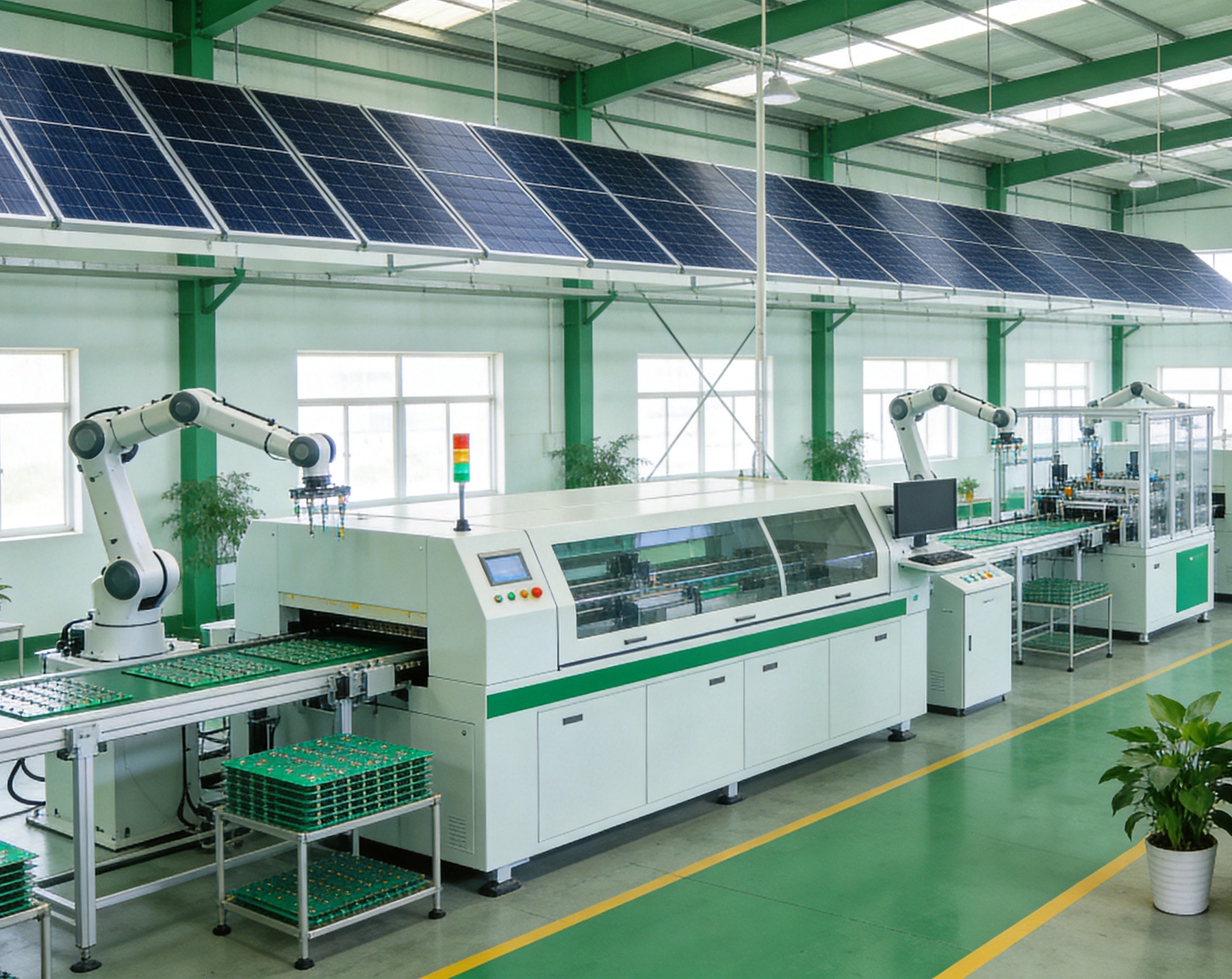
The carbon footprint of PCB fabrication extends beyond electricity use. Process heat generation often uses fossil fuels. Chemical production, transportation, and disposal all add lifecycle impacts. While energy efficiency improvements reduce some impacts, the fundamental energy requirements of Pcb Manufacturing remain substantial, driving interest in both efficiency and renewable energy adoption.
PCB fabrication inherently involves subtractive processes—unwanted copper is etched away, laminates are drilled and milled, and boards are finished with various coatings. These processes generate substantial waste: etched copper, drilled laminate scraps, off-cuts, and processing materials. For every square foot of finished board, several additional square feet of material may be consumed in processing.
While much of this material can be recycled or recovered, collection, sorting, and processing requires energy and infrastructure. Some materials like certain laminate formulations contain substances that complicate recycling. Material waste represents both environmental impact and economic cost—materials that become waste represent sunk costs that could be reduced through process optimization and material efficiency improvements.
Material innovations address many environmental challenges by eliminating hazardous substances, reducing waste, and enabling better end-of-life options. These materials maintain or improve performance while reducing environmental impact throughout their lifecycle.
Traditional FR-4 laminates contain halogens (bromine and chlorine) that provide flame retardancy but create toxic dioxins and furans when burned. Halogen-free laminates use alternative flame retardant systems—typically phosphorus-based or nitrogen-phosphorus compounds—that provide comparable fire performance without hazardous byproducts. These laminates meet UL 94 V-0 flammability ratings while eliminating halogen content.
The environmental benefits extend beyond end-of-life disposal. Halogen-free laminates reduce toxic emissions during any thermal processing that might occur during manufacturing or use. They simplify recycling because halogen-free materials can be processed through conventional material recovery streams without special handling. Performance-wise, halogen-free laminates provide similar electrical and mechanical characteristics to traditional FR-4, though formulations vary by manufacturer.
While halogen-free materials often cost more than traditional laminates, the price premium has decreased as adoption increases. For manufacturers targeting environmental certifications or serving markets with halogen restrictions, halogen-free laminates provide essential compliance while enabling broader market access.
Lead-based solders dominated electronics assembly for decades, but environmental and health concerns drove industry adoption of lead-free alternatives. Common lead-free alloys include tin-silver-copper (SAC) compositions like SAC305 (96.5% tin, 3.0% silver, 0.5% copper) or SAC405. These alloys provide reliable solder joints without lead's environmental and health hazards.
Lead-free solders require higher processing temperatures—typically 235-260°C compared to 220-240°C for leaded solders. This temperature increase affects thermal processing profiles and may stress temperature-sensitive components. However, the environmental benefits are significant: lead-free solders eliminate lead from electronic waste streams, reduce hazardous material handling requirements, and comply with regulations like RoHS that restrict lead in electronic products.
The industry has adapted to lead-free requirements through component packaging modifications, assembly process changes, and improved thermal management. For new designs, lead-free compatibility is now standard. Legacy components and assemblies requiring leaded solder are increasingly limited to specific applications with formal exemptions from lead-free requirements.
Emerging material developments explore bio-based and recycled content options for PCB substrates. Bio-based laminates incorporate renewable materials like plant-derived resins alongside conventional glass fibers. While not replacing traditional materials entirely, these formulations reduce reliance on petroleum-based components and can provide similar performance characteristics for certain applications.
Recycled content options include recycled copper for foil and recovered materials in laminate formulations. Recycled copper requires less energy to process than primary copper, reducing lifecycle environmental impact. Some laminate manufacturers incorporate recycled glass fibers from other industries, providing market for materials that might otherwise become waste.
These bio-based and recycled content options remain emerging rather than mainstream, but they represent important sustainability directions. As material science advances and production volumes increase, costs will decrease and capabilities will expand, making these options more accessible for broader applications.
Processing chemicals like photoresists, developers, and strippers traditionally contain organic solvents and other compounds requiring special handling. New formulations use water-based chemistries that reduce VOC emissions, simplify waste treatment, and improve worker safety. Water-soluble photoresists, for example, eliminate solvent-based developers and strippers in favor of aqueous solutions that are easier and safer to handle.
Low-toxicity alternatives exist across the PCB fabrication process: non-cyanide gold plating baths, alkaline etching solutions, and formaldehyde-free final finishes among others. These materials reduce hazardous waste generation, simplify treatment requirements, and create safer working environments. Performance characteristics vary by specific formulation and application, but advances in chemistry have brought many low-toxicity options to performance parity with traditional materials.
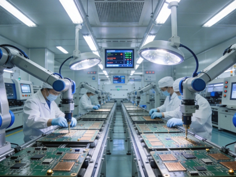
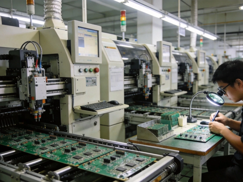
Material improvements alone can't address PCB fabrication's environmental impact—process innovations are equally important. Advanced manufacturing approaches reduce chemical use, energy consumption, waste generation, and water consumption while maintaining or improving quality.
Traditional PCB manufacturing is subtractive—copper is plated then etched away to create circuit patterns. Additive processes build circuits by depositing copper only where needed, eliminating etching entirely. Semi-additive approaches combine elements of both methods, using thin initial copper layers that are built up rather than etched away.
The environmental benefits are substantial. Additive processes eliminate etching chemicals and the hazardous waste they generate. They reduce copper consumption because copper is deposited only where needed. They also eliminate etching steps from the process sequence, reducing water use for rinsing and energy consumption for maintaining etching systems.
While additive processes require different equipment and processing approaches, leading manufacturers increasingly adopt them for high-density applications where they also provide performance advantages. As these technologies mature and scale, their environmental benefits will apply to broader product ranges.
Process optimization reduces environmental impact by making processes more efficient—using less material, energy, and chemicals while maintaining quality. Examples include optimizing etching chemistry concentrations to reduce chemical consumption, refining rinse sequences to minimize water use, and adjusting process parameters to maximize first-pass yields.
Statistical process control (SPC) systems monitor key process parameters continuously, enabling adjustments that maintain optimal conditions rather than allowing process drift that increases material and energy waste. Automated process control systems adjust temperatures, flow rates, and chemistry concentrations in real-time based on measured conditions, maintaining efficiency that would be impossible with manual control.
The cumulative impact of these optimizations can be significant. A 10% reduction in etchant consumption, a 15% reduction in water use, and a 5% improvement in first-pass yield collectively reduce environmental impact while lowering costs. Manufacturers embracing systematic process optimization achieve environmental benefits that also improve profitability.
Water recycling systems treat and reuse process water rather than discharging it after single use. Closed-loop systems capture water from rinsing operations, treat it to remove contaminants, and return it for reuse. Advanced systems achieve 90% or higher water recycling rates, dramatically reducing fresh water consumption and discharge volumes.
Recycling systems vary in sophistication. Simple systems treat water for reuse in non-critical applications like initial rinses. Advanced closed-loop systems produce water quality suitable for all process stages, effectively eliminating discharge except for concentrated waste streams. While these systems require investment and ongoing maintenance, they reduce water acquisition costs and discharge fees while providing environmental benefits.
Water recycling also reduces energy use by reducing the need for heating fresh water to process temperatures. Recycled water often requires less temperature adjustment because it's already closer to process conditions. These combined benefits make water recycling increasingly attractive for manufacturers facing water scarcity or high water costs.
Energy efficiency improvements reduce PCB fabrication's carbon footprint regardless of energy sources. Variable frequency drives on motors, heat recovery systems that capture waste heat, high-efficiency lighting, and optimized HVAC systems all reduce energy consumption. Process-specific improvements like optimized lamination cycles that heat and cool more efficiently also contribute.
Renewable energy adoption further reduces environmental impact. Manufacturers install solar panels, purchase renewable energy credits, or contract for renewable power from utilities. Solar installations on manufacturing facilities provide both cost savings and green energy credentials that resonate with environmentally conscious customers.
Energy management systems monitor consumption patterns across equipment and processes, identifying optimization opportunities. These systems often pay for themselves through reduced energy bills while simultaneously reducing environmental impact. Combined with efficiency improvements, renewable energy can dramatically reduce PCB fabrication's carbon footprint.
Even the most efficient processes generate waste—how that waste is managed determines its environmental impact. Waste reduction strategies minimize generation at source, while material recovery systems extract value from what's generated, creating circular economy approaches rather than linear disposal.
Copper from etching operations, board scrap, and process streams represents significant value and environmental impact. Traditional approaches sent this copper to hazardous waste treatment facilities. Modern recovery systems extract copper from etching solutions for reuse, recover copper from rinse waters, and collect scrap copper for recycling.
Recovery systems include electrolytic copper recovery that plates copper directly from solution onto cathodes for collection, ion exchange systems that capture dissolved copper, and filtration systems that collect particulate copper. Recovered copper meets specifications for reuse in production or sale to metal recyclers, creating revenue streams that offset system costs.
Copper recovery reduces hazardous waste generation, lowers raw material costs, and reduces the environmental impact of primary copper production. For larger fabricators, copper recovery systems often achieve payback periods under two years while significantly reducing environmental footprint.
Drilled laminate scrap, panel off-cuts, and other solid waste traditionally went to landfill. Recovery systems now sort and process these materials for reuse or recycling. Laminate scrap containing copper can be processed through material recovery to extract metals. Clean laminate materials can find reuse in other applications or be recycled for material recovery.
Some manufacturers implement scrap minimization through optimized panel layouts that reduce off-cuts, nesting optimization for irregular shapes, and design for manufacturability reviews that identify waste reduction opportunities. These approaches reduce waste generation while improving material utilization efficiency.
Material sorting systems separate scrap by type and composition, enabling appropriate recycling pathways. Manual sorting for smaller operations, automated systems for larger facilities—both improve material recovery rates and reduce landfill disposal.
Hazardous waste from PCB fabrication includes spent etchants, plating solutions, and process chemicals. Reduction strategies focus on chemical efficiency improvements that extend chemical life, closed-loop systems that minimize discharge, and alternative chemistries that reduce hazardous classifications.
Chemistry optimization maintains etching and plating solution compositions within optimal ranges through continuous monitoring and controlled addition. Extended bath life reduces chemical consumption and hazardous waste generation. Some systems incorporate regeneration processes that restore solution composition without complete bath replacement.
Alternative chemistries replace hazardous materials with less problematic alternatives where possible. Examples include non-cyanide gold plating baths, formaldehyde-free final finishes, and alkaline etching systems with lower environmental impact. While alternative chemistries may require process adjustments, their reduced regulatory burden and waste treatment requirements often make them attractive despite transition costs.
Sustainability initiatives often align with regulatory requirements and voluntary certifications. These frameworks provide structure for sustainability efforts while demonstrating commitment to customers and regulators.
RoHS (Restriction of Hazardous Substances) restricts lead, mercury, cadmium, and other hazardous materials in electronic products, driving lead-free solder and halogen-free material adoption. REACH (Registration, Evaluation, Authorisation and Restriction of Chemicals) regulates chemical substances in the EU market, requiring manufacturers to understand and manage chemical risks throughout product lifecycles.
WEEE (Waste Electrical and Electronic Equipment) establishes collection, recycling, and recovery targets for electronic waste, creating responsibility for end-of-life product management. Regional variations of these regulations exist globally, but the trend toward increasingly stringent environmental requirements is universal.
Compliance with these regulations requires documentation, testing, and sometimes certification processes. However, compliance activities also provide frameworks for systematic environmental management that extend beyond minimum requirements.
ISO 14001 certification demonstrates implementation of systematic environmental management systems. The standard requires organizations to identify environmental aspects, set objectives and targets, implement management programs, and monitor performance. Certification provides third-party verification of environmental management capabilities.
For PCB manufacturers, ISO 14001 often becomes the foundation for broader sustainability initiatives. The systematic approach required by the standard drives identification of improvement opportunities and implementation of management processes that support environmental performance.
Electronics industry certifications like IPC-1401 provide guidance on environmentally sustainable Electronics Manufacturing. While not a certification per se, following IPC-1401 guidance demonstrates commitment to industry best practices for sustainability. Some manufacturers pursue certifications from electronics industry organizations addressing specific environmental aspects.
Forest Stewardship Council (FSC) certification for paper-based packaging and other forestry products complements PCB fabrication sustainability efforts. For manufacturers producing complete electronic products, broader certifications like EPEAT (Electronic Product Environmental Assessment Tool) may apply.
Large customers often impose specific environmental requirements on suppliers. These may include restrictions on specific substances, requirements for particular certifications, reporting requirements on environmental performance, or preference for suppliers with demonstrated sustainability programs.
Meeting customer-specific environmental requirements increasingly becomes a competitive necessity rather than optional differentiation. Manufacturers without robust sustainability programs may find themselves excluded from certain supply chains or markets.
Sustainability initiatives in PCB fabrication aren't just about environmental responsibility—they deliver tangible economic benefits. Cost reductions, risk mitigation, and competitive advantages make sustainability investments increasingly attractive from financial perspectives as well as environmental ones.
Process optimization reduces material consumption, energy use, and waste generation—each representing direct cost reductions. Less chemical consumption per square foot of board reduces material costs. Reduced energy consumption lowers utility bills. Lower waste generation reduces disposal costs. Combined, these reductions can amount to significant cost savings.
Material recovery systems turn waste into revenue streams. Copper from etching solutions, scrap metal from processing, and recovered materials create income that offsets system costs. While recovery systems require investment, payback periods are often short enough to make them financially attractive based on material value alone.
Environmental regulations are becoming more stringent globally, with increasing enforcement and penalties for non-compliance. Proactive sustainability initiatives reduce regulatory risk by staying ahead of requirements rather than reacting after they're imposed. This proactive approach reduces compliance costs and avoids potential penalties or business interruptions.
Supply chain risks also matter. Customers increasingly evaluate suppliers on environmental performance, and poor sustainability performance can result in lost business. Suppliers with strong sustainability programs enjoy competitive advantages in markets where environmental considerations matter to customers.
Environmentally conscious customers—from consumer electronics brands to industrial equipment manufacturers—actively seek suppliers with demonstrated sustainability programs. Strong sustainability credentials become differentiators in competitive markets, providing advantages in winning and retaining customers.
Sustainability messaging resonates with end consumers as well. Products marketed as environmentally friendly appeal to growing consumer segments prioritizing sustainability. While individual PCBs rarely feature in consumer marketing, manufacturers throughout the supply chain benefit from being able to claim environmentally responsible manufacturing practices.
Sustainability trends show no sign of reversing—environmental requirements will continue strengthening, and customer expectations will continue rising. Manufacturers investing now in sustainability capabilities position themselves for long-term competitiveness as requirements evolve. Those delaying investments risk falling behind as sustainability becomes baseline expectation rather than differentiator.
The competitive dynamics of sustainability create opportunities for first movers. Manufacturers establishing leadership positions in sustainable PCB fabrication capture market share and build reputations that pay dividends as environmental considerations grow in importance throughout the electronics industry.
Implementing sustainability initiatives requires systematic approaches that balance benefits with costs and implementation challenges. While every manufacturer's situation differs, certain strategies prove consistently effective across organizations.
Begin sustainability initiatives with comprehensive assessment of current environmental impacts across processes, materials, and facilities. This assessment identifies the most significant environmental aspects and the greatest improvement opportunities. Prioritize initiatives based on environmental impact, implementation feasibility, and expected benefits.
Assessment should include material flow analysis tracking materials through processes, energy audits identifying consumption patterns and efficiency opportunities, water use analysis identifying consumption and discharge patterns, and waste characterization understanding types and volumes of waste generated. This comprehensive baseline enables measurement of improvement over time.
Implement new initiatives through pilot programs before full-scale deployment. Pilots provide opportunities to learn, adjust approaches, and demonstrate value before committing to larger investments. Document lessons learned from pilots to improve full-scale implementation.
Pilots should have clear objectives, success criteria, and timelines. They should involve operators who will eventually use systems or processes at scale. Lessons from pilots—both positive and negative—guide refinement before broader implementation.
Sustainability initiatives succeed or fail based on employee engagement. Operators on the front lines of processes often identify improvement opportunities that management overlooks. Training ensures employees understand sustainability objectives and their role in achieving them.
Recognition programs celebrate sustainability achievements, building momentum and engagement. Cross-functional teams bring together perspectives from operations, quality, engineering, and management. Engaged employees not only implement initiatives but also generate new ideas for further improvements.
Sustainability isn't a destination—it's a journey of continuous improvement. Establish systems for tracking environmental performance metrics, regularly reviewing progress, and identifying new opportunities. Benchmark against industry leaders and best practices to identify gaps and improvement potential.
Technology advances continually create new opportunities for sustainability improvements. Stay informed about emerging technologies and approaches. Regular assessment ensures awareness of new possibilities and readiness to implement when appropriate.
Halogen-free PCB laminates eliminate bromine and chlorine from flame retardant systems, replacing them with phosphorus-based or nitrogen-phosphorus compounds. These materials matter because when halogen-containing laminates burn or undergo thermal decomposition, they release toxic dioxins and furans that are hazardous to human health and the environment. Halogen-free laminates provide equivalent flame retardancy without these hazards, simplifying end-of-life disposal and reducing toxic emissions during any thermal events. They also comply with regulations restricting halogens in electronic products and meet requirements for environmentally sensitive applications.
Cost premiums for sustainable materials vary by specific material and application. Halogen-free laminates typically cost 15-30% more than traditional FR-4, though the premium has decreased as adoption increases. Lead-free solder alloys may cost 10-25% more than leaded alternatives, though processing costs may also increase slightly due to higher operating temperatures. Bio-based and recycled content materials often carry premiums of 20-50% depending on formulations and volumes. However, these premiums don't tell the whole story—sustainable materials may reduce other costs through simplified compliance, reduced waste treatment requirements, and improved market access. Many manufacturers find that total cost impacts are less than material premium differences suggest when considering the entire value chain.
Small fabricators can pursue sustainability despite limited resources by focusing on high-impact, low-cost initiatives initially. Process optimization through SPC and parameter tuning reduces waste and consumption with minimal capital investment. Water recycling can start with simple systems for specific applications before expanding. Chemical optimization extends solution life without major equipment changes. Small facilities can also share services like waste treatment through cooperative arrangements. While some initiatives like copper recovery systems or renewable energy installations require capital, smaller facilities can access financing, grants, or incentives that improve payback economics. The key is prioritizing initiatives based on impact and feasibility, then scaling as resources allow.
ISO 14001 provides the foundational environmental management certification most manufacturers should target. Beyond this, certification choices depend on specific markets and customer requirements. For manufacturers serving automotive or medical markets, compliance with industry-specific environmental standards may be required. For those in regulated markets like EU, demonstrating compliance with RoHS, REACH, and other directives is essential. Some customers require IPC-1401 implementation or similar industry guidance. The practical approach is to identify customer and market requirements, then pursue certifications that meet those needs while building broader environmental management capabilities through ISO 14001 or similar frameworks.
Modern sustainable PCB materials and processes maintain or improve product performance compared to traditional alternatives. Halogen-free laminates provide electrical and mechanical characteristics comparable to standard FR-4. Lead-free solders create reliable solder joints, though the higher processing temperatures require appropriate component selection. Additive processes can provide finer features and better electrical performance than subtractive approaches in some applications. Water-soluble processing materials deliver comparable results to solvent-based alternatives when properly formulated. While early sustainable materials sometimes had performance limitations, advances in material science have largely eliminated these issues. In many cases, sustainable alternatives actually improve performance through reduced contamination, better process control, or enhanced material characteristics.
Sustainability in PCB fabrication has evolved from regulatory burden to competitive advantage. Environmental regulations, customer expectations, and market dynamics create strong drivers for sustainable practices. But beyond compliance requirements, sustainability initiatives deliver economic benefits through cost reductions, risk mitigation, and market differentiation.
Material innovations provide halogen-free laminates, lead-free solders, bio-based components, and low-toxicity processing materials. Process improvements enable additive manufacturing, closed-loop water systems, energy efficiency, and waste reduction. Recovery systems extract value from waste streams that previously created disposal costs. Together, these advances transform PCB fabrication's environmental profile.
For manufacturers, the path forward involves systematic assessment, prioritized implementation, employee engagement, and continuous improvement. Sustainability becomes integrated into business operations rather than treated as separate initiatives. The result—reduced environmental impact, improved economics, and enhanced competitiveness—makes sustainability not just environmentally responsible but strategically essential.
As environmental considerations continue growing in importance throughout the electronics industry, sustainable PCB fabrication capabilities will become baseline expectations rather than differentiators. Manufacturers investing now position themselves for future success while addressing current environmental challenges. The combination of environmental responsibility and business value makes sustainability one of the most compelling trends reshaping PCB fabrication today.

Detailed Explanation of the Types, Materials, and Applications of Flexible Circuit Boards 101June/04/2026

What is Rigid-Flex PCB? Complete Guide from China ManufacturerMay/18/2026
HDI PCB Manufacturing Process: Step-by-Step ExplanationMay/13/2026

The Future of PCB Manufacturing in China: Trends for 2026 and BeyondMay/19/2026
The Complete Guide to SMT PCB Assembly in ChinaJune/17/2026
What is HDI PCB? A Complete Guide from China HDI PCB ManufacturerMay/13/2026

What is Metal Core PCB? Complete Guide from China ManufacturerMay/18/2026
Why Choose a China HDI PCB Manufacturer for Your Project?May/13/2026