Open Nav
Smartphones have become progressively thinner over the past decade, with flagship devices measuring under 7 millimeters in thickness despite incorporating more functionality than ever before. Tablets follow the same trend, delivering laptop-class performance in chassis that seem impossibly thin. This miniaturization trend extends far beyond careful mechanical design and component selection—the printed circuit boards inside these devices represent the unsung enablers of modern slim form factors. HDI (High Density Interconnect) Pcb Technology has evolved from a specialized capability to the foundation of mobile electronics, with Apple's adoption of Any-layer Hdi in iPhones marking the transition from innovation to industry standard.
Understanding how HDI Pcb Technology enables slim device design reveals the intersection of materials science, precision manufacturing, and electrical engineering that makes modern smartphones possible. The combination of laser-formed microvias, fine-line routing, and Sequential Lamination provides routing densities unattainable through conventional PCB construction, allowing designers to pack complete computer systems into volumes measured in cubic centimeters.
The first generation of iPhones measured 12.3 millimeters thick—a dimension considered impressive for 2007 but impossibly bulky by contemporary standards. Each subsequent generation has reduced thickness incrementally, with iPhone 6 reaching 6.9 millimeters, iPhone 12 at 7.4 millimeters, and modern flagship devices averaging below 7 millimeters despite larger screens and more powerful processors. This thickness reduction follows Moore's Law-like progress in PCB density, as each halving of board area requires roughly doubling of routing density to accommodate the same circuitry.
Thickness reduction benefits extend beyond aesthetic appeal to practical advantages including improved ergonomics, reduced material costs, and the ability to incorporate larger batteries within the same external dimensions. Consumers perceive thinner devices as more technologically sophisticated, driving manufacturer investment in the technologies that enable slim form factors. The competitive pressure has accelerated Hdi Pcb adoption beyond the premium segment, with mid-range devices now incorporating advanced constructions that were flagship technology just a few years ago.
While devices have become thinner, their functionality has expanded dramatically. Modern smartphones include capabilities that were unimagined a decade ago: multiple cameras with optical image stabilization, 5G connectivity with multiple frequency bands, wireless charging, depth sensing arrays, and displays with higher resolution than desktop monitors from the early 2000s. Each new feature adds circuitry that must fit within continuously shrinking volume budgets, creating a relentless pressure for increased routing density.
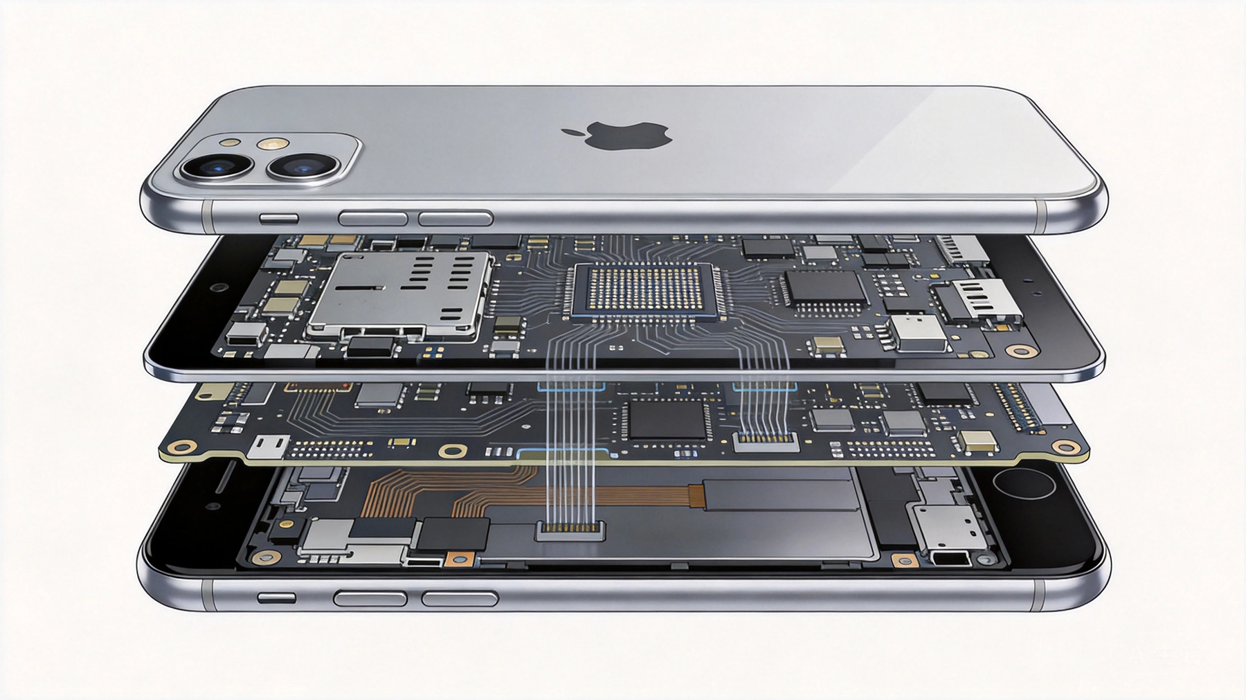
The combination of reduced thickness and increased functionality creates what seems like an impossible design problem: how to fit more circuitry into less space. The answer lies in Hdi Pcb technology, which provides routing densities several times higher than conventional multilayer boards through microvias that connect layers without consuming routing channels through the entire board thickness. This capability enables three-dimensional routing that would be impossible with standard through-hole vias.
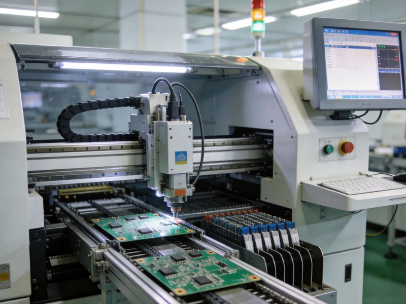
Microvias represent the core enabling technology of HDI construction. Laser-ablated holes below 0.15 millimeter diameter connect adjacent layers in the PCB stackup, creating interconnection points that occupy minimal area compared to conventional through-hole vias. These microvias typically have depth equal to one dielectric layer thickness, creating connections between layers without the holes extending through the entire board that would block routing on intermediate layers.
The laser ablation process using CO2 or UV lasers provides precise control over hole dimensions and placement accuracy. CO2 lasers efficiently ablate organic dielectric materials including FR-4 and polyimide but require a copper etch mask or conformal mask to define via locations. UV lasers can directly drill through thin copper foils in addition to dielectric, enabling a more streamlined process flow for certain constructions. Both laser types achieve placement accuracy below 20 micrometers, essential for the fine-pitch components common in mobile devices.
Microvia filling with conductive material creates reliable electrical connections with low resistance. The most common approach uses copper electroplating to fill the microvia, creating a solid copper connection through the dielectric thickness. This plating process simultaneously metallizes the via barrel and builds up copper on the board surface, creating conductive paths with low resistance suitable for both signal and power connections.
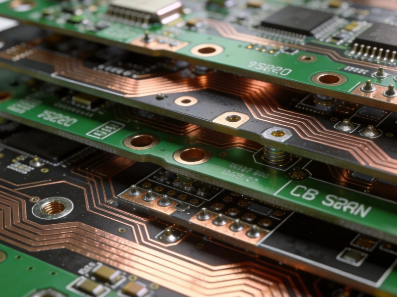
HDI boards are built using Sequential Lamination, where pairs of layers are laminated, drilled, and plated before adding additional layer pairs. This process differs from conventional multilayer board construction where all layers are laminated simultaneously in a single press operation. Sequential lamination enables microvia connections between layers in ways that single-press construction cannot achieve, particularly for Any-layer Hdi where microvias connect any combination of adjacent layers.
The sequential build-up process begins with the core layers—typically 2 or 4 layers—that form the central stackup. Each subsequent lamination adds a dielectric layer, Copper Foil, and microvias connecting to the previous structure. This layered approach enables complex via structures that would be impossible to manufacture in a single operation, including microvias connecting different depth levels within the stackup.
Any-layer HDI takes sequential lamination to its logical extreme, enabling microvias between any adjacent layers throughout the stackup. This capability maximizes routing density by eliminating the requirement that microvias follow a consistent pattern through the stackup. The trade-off is increased manufacturing complexity and cost, making any-layer HDI primarily suitable for high-volume applications where the additional cost is justified by performance requirements.
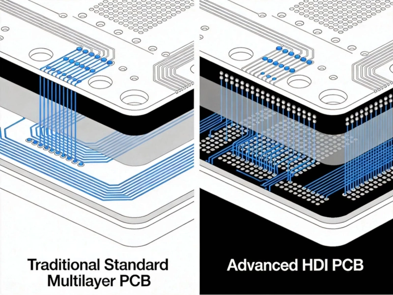
The primary advantage of HDI construction is routing density several times higher than equivalent standard boards. Conventional through-hole vias consume routing channels through all intermediate layers, effectively blocking space that could otherwise carry signals or power. Microvias occupy minimal area and connect only adjacent layers, freeing up space for routing on intervening layers and enabling three-dimensional routing approaches that exploit the full stackup depth.
For smartphones where board area may measure just 50mm by 70mm, every square millimeter counts. HDI constructions can achieve 50% to 70% higher routing density than equivalent standard boards, enabling more circuitry within the same footprint. This density gain allows designers to incorporate features that would be impossible with conventional PCB technology while maintaining the thin form factors that modern smartphones and tablets require.
HDI manufacturing enables finer trace and space geometries than conventional PCB processes achieve reliably. Line/space pairs of 0.075mm/0.075mm are routine for HDI constructions, compared to 0.1mm/0.1mm for standard boards. This finer pitch enables more routing channels between pins of fine-pitch BGA packages and between component bodies, increasing routing density without requiring additional board layers.
Dielectric thickness in HDI boards is often reduced compared to standard constructions, with dielectric thicknesses below 0.1mm typical for the thin cores used in sequential lamination. Thinner dielectric enables tighter coupling between layers for differential pairs, reducing the width required for controlled impedance traces. While thinner dielectric can increase crosstalk between adjacent layers, careful signal layer assignment and ground plane spacing mitigate this concern in properly designed mobile devices.
Blind vias connect an outer layer to one or more inner layers without reaching the opposite outer surface, while buried vias reside entirely between inner layers. These structures consume less board thickness than through-hole vias while providing the electrical connectivity needed for complex designs. For mobile devices where thickness is constrained, blind and buried vias reduce the effective PCB thickness compared to equivalent through-hole designs.
The combination of blind and buried vias with microvia technology enables routing strategies that fully exploit three-dimensional space. Signals can route on any layer and transition between layers at multiple points using vias that do not extend through the entire board thickness. This flexibility is essential for the complex routing requirements of modern smartphones, where multiple high-speed interfaces, power distribution networks, and sensitive analog circuits must coexist in a compact volume.
Mobile device PCBs often use thin-core constructions to minimize overall board thickness. Cores as thin as 0.05mm enable HDI stackups with total thickness below 0.5mm for 8 to 10 layer constructions, compared to 1.0mm or more for equivalent standard boards. This thickness reduction directly contributes to slimmer device form factors, with each millimeter of board thickness reduction representing valuable space for batteries, displays, or simply overall device thinning.
Thin laminate materials present manufacturing challenges that require specialized handling and processing. The flexible nature of thin cores makes them susceptible to damage during handling, requiring transport frames and automated material handling equipment. Processing parameters for lamination, etching, and drilling must account for the reduced thickness and increased flexibility compared to standard laminates.
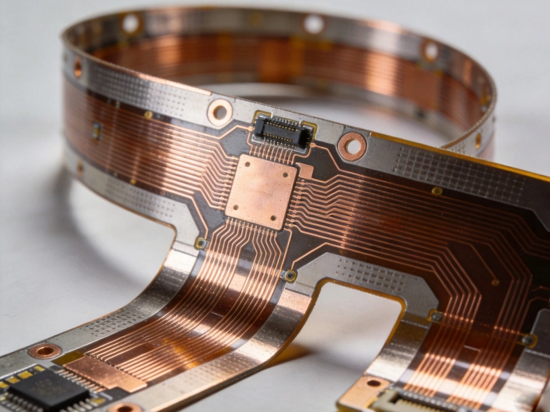
Many smartphones and tablets incorporate rigid-flex constructions that combine rigid PCB sections with flexible interconnects to enable folding, sliding, or hinging mechanisms while maintaining high routing density. Rigid-flex boards enable device architectures impossible with all-rigid PCBs, allowing displays to fold, cameras to swivel, or keyboards to slide out from within a device chassis.
The flexible sections of rigid-flex boards use polyimide or other flexible dielectrics that can bend thousands of times without electrical failure. Transition zones between rigid and flexible sections receive special design attention to manage stress concentrations that could cause copper cracking or delamination. These transition zones often include stiffener materials and restricted bend radii to ensure long-term reliability through the mechanical stresses mobile devices experience during use.
Mobile devices incorporate multiple high-speed serial interfaces including MIPI for displays, PCIe for peripheral connections, and high-speed USB for data transfer. These interfaces require controlled impedance transmission lines with consistent performance across the operating frequency range. Low-Dk dielectric materials with stable electrical properties across temperature enable more predictable impedance and reduced signal loss compared to standard FR-4.
High-speed mobile interfaces often target 10GHz operation or higher, requiring dielectrics with loss tangents below 0.004 to maintain acceptable signal integrity. While FR-4 can work with careful design, specialized materials including hydrocarbon ceramics and modified FR-4 formulations provide better performance margins. The additional cost of these materials is justified in premium smartphones where signal integrity directly affects device performance and customer satisfaction.
Modern smartphones and tablets utilize fine-pitch BGAs with ball pitches of 0.4mm or below, along with CSP (Chip Scale Package) devices with pitches down to 0.3mm. These components require placement accuracy below 0.015mm to achieve acceptable assembly yields. HDI boards with their microvia infrastructure and precise registration tolerances provide the necessary foundation for reliable fine-pitch component assembly.
Placement equipment for fine-pitch components uses high-resolution cameras that can resolve features below 10 micrometers, enabling accurate component placement despite the microscopic dimensions of the component packages. The relationship between PCB hole registration accuracy and component placement accuracy means HDI manufacturing capabilities directly enable fine-pitch component utilization.
Thin mobile devices provide limited thermal conduction paths for heat generated by processors, power management ICs, and wireless transceivers. The thin PCB construction provides limited mass for heat absorption, and the device enclosure often hampers convection cooling. HDI boards must incorporate thermal management features including thermal vias, metal core sections, and interface materials that conduct heat toward the device exterior or into the chassis for dissipation.
Thermal vias concentrated beneath high-power components provide conductive paths to the opposite side of the board, where the heat can spread into the device enclosure or external heatsink surfaces. Metal core sections or thermal coins embedded in the PCB stackup provide localized high-conductivity paths for particularly challenging thermal conditions. These thermal management features increase board complexity but are essential for reliable performance in slim device form factors.
Mobile devices utilize components specifically engineered for low-profile installations. Thin-profile connectors, recessed component packages, and surface-mount devices with low heights all contribute to minimizing overall device thickness. Some components including cameras, sensors, and connectors include mounting features that integrate directly with the PCB stackup to avoid adding height beyond the board thickness.
The combination of HDI PCB technology and component selection for low-profile mounting enables designers to minimize total board thickness while maintaining electrical performance. Careful component placement optimization ensures that the tallest components align with locations where device thickness constraints allow additional vertical space, with flexible sections accommodating components that cannot fit within the rigid board envelope.
A modern flagship smartphone might utilize a 10-layer HDI stackup with the following approximate layer assignment: Layer 1 (Top) for component placement and signal routing, Layer 2 as ground plane, Layers 3-6 for internal signal routing and power distribution, Layer 7 as ground plane, and Layer 8 (Bottom) for additional component placement and routing. Microvias connect adjacent layers throughout the stackup, with through-hole vias used only where connections must span multiple layer pairs.
Any-layer HDI construction enables microvia placement flexibility that optimizes routing density. Signal layers alternate between routing and reference planes to maintain controlled impedance and minimize crosstalk. Power distribution networks utilize inner layers with heavier copper to reduce voltage drop while maintaining overall board thickness constraints.
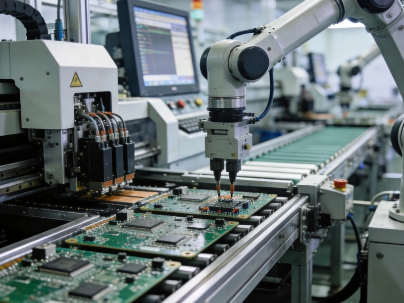
The smartphone's main processor typically occupies the largest component area, surrounded by supporting ICs including memory, power management, and connectivity devices. The dense placement of these components requires routing channels both between components and through the component pads themselves using microvias that access inner routing layers. The combination of fine-pitch component packaging and HDI routing enables placement densities exceeding 80 components per square centimeter for complex mobile devices.
High-speed interfaces route as differential pairs with controlled impedance, using adjacent layers as reference planes. The tight coupling enabled by thin dielectric spacing reduces the trace width required for target impedance, saving routing space while maintaining signal integrity. Ground stitching vias placed at regular intervals ensure consistent reference plane potential and reduce crosstalk between adjacent signal lines.
Device thickness continues trending downward, with some manufacturers exploring sub-6 millimeter thicknesses for flagship smartphones. Achieving these targets requires PCB thickness reductions beyond current any-layer HDI capabilities. Approaches under investigation include substrateless PCB constructions where components mount directly to a metal frame with embedded interconnects, and hybrid approaches combining conventional PCB sections with advanced interconnect technologies.
Flexible displays and foldable devices create additional Pcb Design challenges, requiring circuits that bend repeatedly without failure. Advanced flexible materials with improved mechanical properties, new strain relief techniques, and optimized layer stacks that minimize bending stress represent areas of active development. The PCB community is learning to design electronics that accommodate mechanical flexure as a design parameter rather than an exception.
Semiconductor packaging increasingly adopts chiplet architectures that combine multiple specialized silicon dies in a single package. These advanced packages create unique challenges for PCB integration, as the I/O density and thermal characteristics differ from conventional packages. HDI PCB technology evolves to accommodate these packaging innovations, with modified microvia structures, advanced thermal management features, and new layer count optimizations that account for chiplet-specific requirements.
High Density Interconnect Pcb technology represents the foundational technology that enables the slim smartphones and tablets consumers expect from modern mobile devices. Without the routing density, layer count flexibility, and design freedom that HDI provides, incorporating the functionality of contemporary devices into slim chassis would be impossible. The combination of laser-formed microvias, sequential lamination, fine-line routing, and advanced materials creates a platform that continues pushing the boundaries of what can fit within a mobile device volume.
As device requirements continue evolving with higher performance, new features, and thinner form factors, HDI PCB technology evolves to meet these challenges. Any-layer HDI has become the standard for premium devices, and construction techniques that were experimental a decade ago now represent baseline expectations for mid-range smartphones. The relationship between PCB capability and device form factor ensures that advances in Hdi Technology will continue driving innovation in mobile electronics for the foreseeable future.
HDI constructions with thin cores can achieve 30% to 50% thickness reduction compared to equivalent standard multilayer boards. A 10-layer HDI board might measure 0.5mm thick compared to 1.0mm for a standard board, directly contributing to slimmer device form factors without sacrificing electrical functionality.
Any-layer HDI enables microvias between any adjacent layers throughout the PCB stackup, maximizing routing density by eliminating constraints on where microvias can connect. This capability provides design flexibility essential for the complex routing requirements of modern smartphones, particularly for flagship devices where every millimeter of board area matters.
Microvias typically measure below 0.15mm diameter compared to 0.25mm or larger for standard through-hole vias. More importantly, microvias connect only adjacent layers, consuming minimal board thickness and blocking routing only on the two layers they directly connect. This enables three-dimensional routing impossible with through-hole constructions.
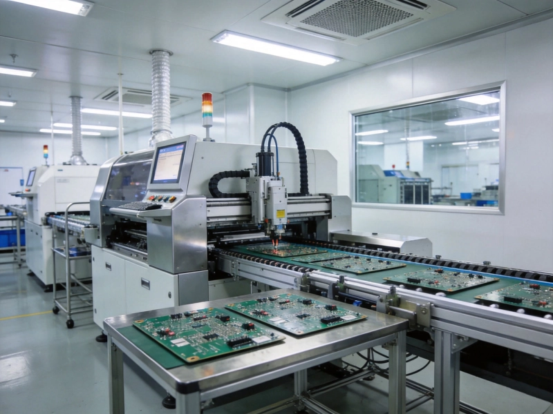
Standard PCB manufacturers generally lack the laser drilling equipment and sequential lamination processes necessary for HDI production. Specialized HDI manufacturers with dedicated equipment and process expertise produce these boards, and quality varies significantly between facilities with different capability levels. Smartphone manufacturers work with established HDI suppliers with proven capability for high-volume production.
HDI boards typically cost 1.5x to 3x equivalent standard boards depending on complexity and layer count. Any-layer HDI commands higher pricing than simpler HDI constructions. However, for smartphones and tablets, the cost premium is justified by the ability to achieve necessary functionality within thin form factors. Standard PCB alternatives simply cannot achieve the required routing density.
HDI PCB vs Standard PCB: Key Differences ExplainedMay/13/2026

Top 10 DFM Tips to Avoid Errors in Your Next PCB OrderJune/18/2026
What is Metal Core PCB? Complete Guide from China ManufacturerMay/18/2026

Finding the Right China Flexible PCB Manufacturer for Wearable TechJune/12/2026
Understanding HDI PCB Technology: A Comprehensive Guide for BeginnersMay/13/2026
SMT PCB Assembly China: A Complete Guide for Global BuyersMay/18/2026
Need It Fast? The Benefits of a Quick Turn PCB Manufacturer in ChinaJune/16/2026
Top 5 Applications of HDI PCBs in Modern ElectronicsMay/13/2026