Open Nav

The Internet of Things has fundamentally changed how we think about electronic devices. From smart home sensors to industrial monitoring equipment, IoT devices are everywhere, and they share one critical requirement: their printed circuit boards must be both small and affordable. This creates unique challenges for engineers and product teams who need to develop prototypes quickly without breaking the bank.
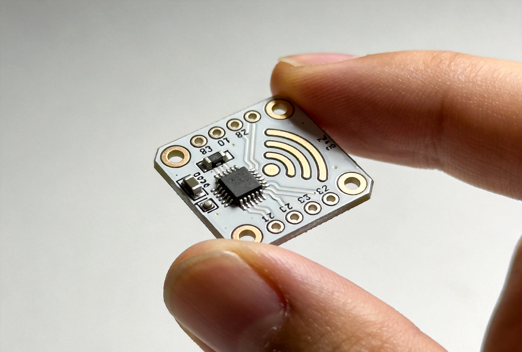
IoT devices operate under constraints that traditional electronics simply do not face. They must be compact enough to fit into everyday objects, energy-efficient to run on batteries for months or years, and inexpensive enough to make high-volume production economically viable. These requirements directly impact Pcb Design and manufacturing decisions.
When you look at a typical IoT sensor or smart device, the PCB inside might be no larger than a few square centimeters. Yet it must contain a microcontroller, wireless transceiver, power management circuitry, and various passive components. Getting all of this to fit while maintaining Signal Integrity and manufacturability requires careful planning.
One of the first challenges in Iot Pcb Design is achieving the required form factor. Designers often turn to High-density Interconnect (HDI) technology, which allows for smaller vias, finer trace widths, and more routing layers in a smaller area. HDI boards can reduce PCB footprint by 30-40% compared to traditional multilayer designs, making them ideal for space-constrained IoT applications.
Component selection also plays a crucial role. Many IoT designs now use 0201 or even 01005 passive components instead of the larger 0402 or 0603 sizes. While these tiny components save space, they require manufacturers with advanced pick-and-place capabilities and strict process control during assembly.
The economics of IoT devices are brutal. When you are producing millions of units, every cent matters. A PCB that costs an extra dollar per unit becomes a multi-million dollar expense across the production run. This cost sensitivity extends to prototypes as well, as design teams need to iterate quickly without accumulating massive NRE (non-recurring engineering) charges.
Low-cost PCB prototypes for IoT have become a specialized service category. Manufacturers offering these services typically use standardized material sets, optimized panel utilization, and streamlined processes to keep per-unit costs down. The trade-off is often longer lead times or more limited design options, but for early-stage development, these constraints are acceptable.
Most IoT devices communicate wirelessly, whether through WiFi, Bluetooth, Zigbee, LoRa, or cellular protocols. Integrating the radio frequency section with the digital circuitry presents unique challenges. Antenna placement, ground plane requirements, and RF shielding all affect both performance and cost.
Some designers choose modules with integrated radios, which simplify the design but add component cost. Others prefer to implement the RF section directly on the PCB, which requires more expertise but can reduce overall BOM cost at high volumes. For prototypes, integrated modules often make sense because they reduce development time and risk.
IoT devices frequently run on batteries, making power efficiency paramount. This affects everything from component selection to PCB layout. Low-power microcontrollers, efficient voltage regulators, and careful attention to sleep mode current draw all contribute to longer battery life.
From a PCB perspective, power delivery networks must be designed with low noise and minimal voltage drop. This often means using dedicated power planes, careful decoupling capacitor placement, and wide traces for high-current paths. While these considerations add complexity, they are essential for reliable IoT operation.
Heat Dissipation becomes more difficult as boards get smaller. Components that would have adequate thermal margin in a larger design may overheat in a compact Iot Pcb. Thermal vias, copper pours, and strategic component placement help manage heat, but they also impact manufacturing cost and design flexibility.
For prototypes, thermal issues are sometimes discovered only during testing. Building test fixtures that can measure thermal performance early in development helps identify problems before they become expensive to fix. Some contract manufacturers offer thermal simulation services that can predict hotspots before the first prototype is built.
One of the most effective ways to reduce prototype costs is using standardized manufacturing processes. Many PCB shops offer low-cost prototype services based on fixed panel sizes, standard material grades (typically FR-4), and limited layer counts (usually 2-6 layers). These constraints keep tooling costs low and allow for quick turnaround.
For IoT applications, a 4-layer board often provides the right balance between cost and performance. The outer layers handle component mounting and RF routing, while the inner layers distribute power and ground. This stackup is well-understood by most manufacturers, resulting in consistent quality and competitive pricing.
When ordering larger prototype quantities, panel utilization becomes important. Designing PCBs as arrays or panels allows manufacturers to build multiple units in a single process, spreading setup costs across more boards. This technique is standard in production but can also benefit prototype orders when the design allows.
Some manufacturers have optimized their processes specifically for small IoT devices, offering rates based on "square inches per month" rather than individual board pricing. This model encourages designers to prototype frequently and iterate quickly, which ultimately leads to better products.
Standard FR-4 works well for most IoT prototypes, but some applications require specialized materials. High-frequency IoT devices using sub-6 GHz or millimeter-wave bands may need Rogers or similar high-performance laminates. These materials cost significantly more than FR-4 and often require longer lead times.
For cost-sensitive IoT applications, designers should evaluate whether the performance benefits of specialized materials justify the expense. In many cases, careful layout techniques can achieve adequate performance with standard materials, especially at prototype volumes where cost matters more than marginal performance improvements.
Speed matters in the IoT market. Products that launch first often capture market share that competitors cannot recover. This pressure drives demand for Rapid Prototyping services that can deliver functional boards in days rather than weeks.
Quick-turn Pcb services have responded by offering increasingly fast delivery options. Some manufacturers now promise 24-hour or even same-day turnaround for simple boards. While these expedited services cost more, they can be invaluable when development schedules are tight.
Working with manufacturers early in the design process helps avoid costly surprises. Many Iot Pcb manufacturers offer Dfm (Design For Manufacturing) reviews that identify potential issues before production. This collaborative approach reduces prototype iterations and speeds overall development.
Dfm feedback might address issues like minimum trace widths for the manufacturer's capabilities, component spacing requirements for assembly, or via specifications that affect reliability. Incorporating this feedback early results in prototypes that work correctly the first time, saving both money and schedule.
Component availability has become a significant concern for IoT developers. The semiconductor shortages of recent years demonstrated how supply chain disruptions can derail product development. Designing with readily available components and maintaining buffer stock of critical parts helps mitigate this risk.
Some prototype manufacturers offer component sourcing as part of their service. They maintain relationships with distributors and can often obtain parts faster than individual companies. While this adds cost, it removes the burden of managing multiple vendor relationships during development.
Every design decision involves trade-offs. More layers improve routing flexibility but increase cost. Smaller components save space but require more precise manufacturing. Higher-speed materials enable better RF performance but cost more and have longer lead times. Navigating these trade-offs requires experience and clear priorities.
For most IoT applications, starting with a conservative design and upgrading only where needed makes sense. This approach minimizes initial prototype costs and allows optimization based on actual test results rather than theoretical predictions. Premature optimization often leads to overly complex designs that are difficult to manufacture and debug.
Prototype PCBs must be thoroughly tested before moving to production. This includes functional testing, RF performance validation, thermal testing under load, and reliability screening. Building comprehensive test plans early in development ensures that prototype phases produce actionable data.
Some manufacturers offer testing services as part of prototype orders. This can include basic electrical testing, X-ray Inspection for hidden solder defects, and even Environmental Testing. While these services add cost, they provide confidence that the design is ready for production.
The IoT market continues to evolve rapidly, driving new requirements for Pcb Technology. Smaller devices, longer battery life, faster wireless speeds, and lower costs remain the dominant trends. Meeting these requirements will demand continued innovation in both design techniques and manufacturing processes.
Emerging technologies like embedded components, advanced substrates, and additive manufacturing may eventually transform how IoT PCBs are built. For now, however, the industry continues to rely on incremental improvements to existing processes, squeezing more performance and lower cost from established technologies.
The demand for compact, low-cost PCB prototypes shows no signs of slowing. As IoT devices become more prevalent and competitive, the ability to develop and iterate quickly becomes a critical success factor. Understanding the trade-offs involved in Iot Pcb Design helps engineers make informed decisions that balance performance, cost, and Time-to-market.
Working with experienced manufacturers who understand IoT requirements can significantly improve prototype outcomes. Their expertise in Design For Manufacturing, component sourcing, and rapid turnaround helps teams bring products to market faster and more reliably. In the fast-moving IoT space, that advantage can make all the difference.
IoT Pcb Prototype costs vary widely based on complexity, layer count, and turnaround time. Simple 2-layer boards might cost $10-50 per unit in small quantities, while complex multilayer HDI boards can cost several hundred dollars each. Quick-turn services typically command premium pricing.
Standard prototype lead times range from 5-15 business days depending on manufacturer and complexity. Quick-turn services can deliver boards in 24-72 hours for additional fees. Complex multilayer or HDI boards may require 3-4 weeks even for prototypes.
The most frequent issues include RF performance problems (especially Antenna Integration), Thermal Management in compact spaces, component availability delays, and DFM violations that require respins. Early engagement with manufacturers helps identify and address these challenges.
No, Hdi Technology is beneficial but not always required. Many IoT devices can be successfully implemented on standard multilayer boards with careful design. HDI becomes more important when board size is severely constrained or when very high component density is needed.
Strategies for Cost Reduction include designing for standard manufacturing capabilities, using readily available components, optimizing panel utilization, and avoiding expedited services unless absolutely necessary. Building prototypes in batches rather than individually also reduces per-unit costs.
10 Questions to Ask Your Potential PCB Prototype Manufacturer in ChinaJuly/07/2026
PCB Prototype Pricing Models: Panelization and Setup Fees ExplainedAugust/12/2026
Evaluating a China Multilayer PCB Manufacturer: Certifications and CapabilitiesSeptember/11/2026

How We Handle Intellectual Property Protection for Overseas ClientsOctober/19/2026
PCB Prototype Manufacturing in China: Complete GuideMay/18/2026
Bridging the Gap: Moving from PCB Prototype to Mass ProductionOctober/09/2026
Sourcing Metal Core PCBs for Automotive LED HeadlightsJuly/25/2026
How to Specify Bend Radius for Flexible PCB OrderAugust/06/2026