
Rigid-flex PCBs have become essential in modern electronics, enabling three-dimensional packaging solutions for wearables, medical devices, aerospace systems, and foldable consumer electronics. However, designing these hybrid boards presents unique challenges that differ significantly from traditional Rigid Pcb layouts. Many engineers underestimate the complexity of rigid-flex design, leading to costly manufacturing issues and field failures.
Design For Manufacturing (Dfm) is critical for rigid-flex PCBs because the interaction between mechanical stress, thermal cycling, and electrical performance creates failure modes that do not exist in rigid boards. Statistics from manufacturing facilities indicate that approximately 68% of early failures in rigid-flex boards originate from copper cracking in bend regions, with over 42% directly related to improper coverlay selection or window opening misalignment. Understanding these common mistakes can save manufacturers significant rework costs and prevent product failures in the field.
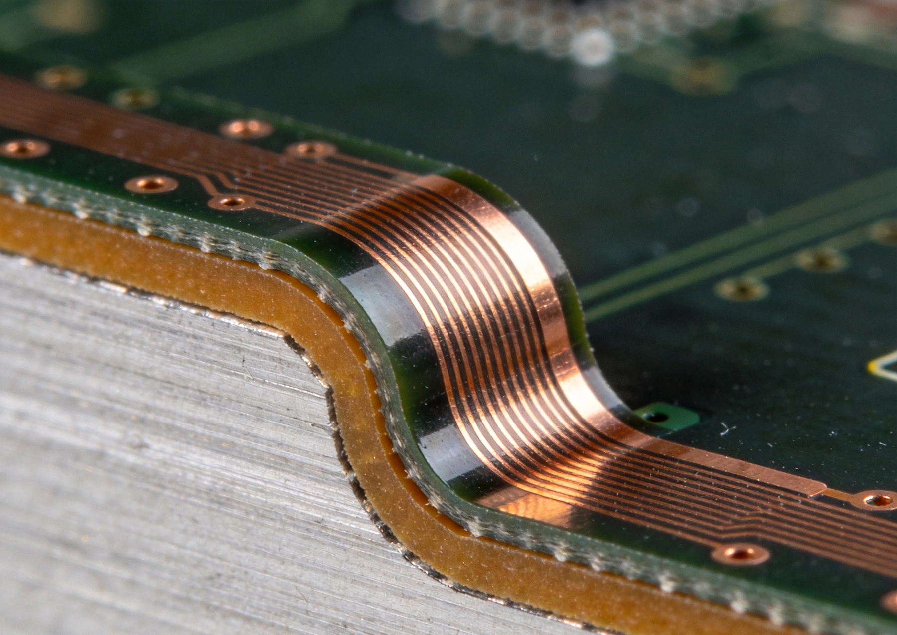
One of the most fundamental mistakes in Rigid-flex Pcb layout is underestimating the importance of Bend Radius. The minimum Bend Radius determines how tightly the flexible section can fold without damaging copper traces or delaminating layers. According to IPC-2223 standards, static bend applications require a minimum bend radius of at least 6 times the total flexible layer thickness, while dynamic bend applications require 100 times the thickness for single-layer circuits.
Designers frequently use the simplified formula R_min = k × T_composite, where k is the multiplier based on application type and layer count. For dynamic applications with continuous flexing, the multiplier must be significantly higher than static applications. Failing to calculate the correct bend radius leads to premature copper fatigue, trace cracking, and delamination failures. Engineers should always verify their calculations against IPC-2223E specifications and consider the total stackup thickness including all copper layers, dielectric materials, and coverlay.
Plated through-holes in bend zones represent one of the most critical Dfm violations in rigid-flex design. Vias create rigid stress concentration points that dramatically increase the likelihood of copper barrel cracking under flexural loading. The mechanical boundary between rigid and flexible sections introduces unique stress patterns that standard Pcb Design rules cannot address adequately.
Ipc Standards and industry best practices mandate a minimum keep-out distance of 1.27mm (50 mils) from any transition boundary, with the industry norm recommending 3.175mm (125 mils) for high-reliability applications. Some designers mistakenly believe that small Microvias pose less risk, but any plated through-hole in a bend zone creates a mechanical discontinuity that concentrates stress. The solution involves relocating all vias to rigid sections and using blind or Buried Vias strategically positioned away from stress zones.
Material selection for flexible regions requires careful consideration of Copper Foil properties. Electrodeposited (ED) copper, which has a columnar grain structure, cracks easily under mechanical deflection. Rolled-annealed (RA) copper features a lamellar grain structure that can withstand 20-40% elongation without fracturing. Many designers fail to specify RA copper for Dynamic Flex zones, leading to premature failure.
The choice between adhesive-based and adhesiveless constructions also impacts reliability significantly. Adhesive-based materials use acrylic layers that exhibit high Z-axis coefficient of thermal expansion (CTE), causing barrel cracking and inner-layer separation during reflow processes. Adhesiveless constructions cast polyimide resin directly onto copper, providing superior thermal stability and flexural endurance. For high-frequency applications above 5GHz or designs requiring reflow compatibility, adhesiveless laminates with RA copper are strongly recommended.
Coverlay serves as the primary protection and insulation layer for Flexible Circuit regions. Window openings in coverlay must provide adequate clearance for solder pads while maintaining sufficient overlap to prevent stress concentration. A common mistake involves designing window openings that are too tight, causing coverlay to overlap pad edges insufficiently and creating reliability issues during assembly and flexing.
Industry standards recommend coverlay overlap into rigid areas of at least 1.0mm (40 mils), with 2.0mm (80 mils) preferred for high-reliability applications. Window openings should extend at least 0.1mm beyond solder pads to accommodate registration tolerances typical of polyimide coverlay lamination processes. Using flexible solder mask (LPI) instead of coverlay in bend regions is another frequent error, as LPI becomes brittle under repeated flexing and will crack, exposing copper to corrosion.
Stackup asymmetry creates internal stresses during lamination and thermal cycling that manifest as board warpage, twist, and coplanarity issues. All layers in a rigid-flex stackup must be mirrored around the central neutral axis, including copper weights, dielectric thicknesses, and material properties. Designers often overlook the importance of balancing copper distribution across all layers.
IPC-2223C requires that adjacent layer copper area differences must not exceed 15% to prevent bow and twist during manufacturing and assembly. Large copper pours on one side of the board without corresponding copper on adjacent layers create unbalanced stress that leads to warpage. When ground planes or power planes are required in flexible regions, cross-hatched patterns with 30-40% copper coverage provide adequate shielding while maintaining flexibility.
Traces crossing bend zones must be routed perpendicular to the bend line to distribute stress evenly. Running traces parallel or diagonal to the bend axis creates non-uniform tensile and shear stresses that accelerate copper fatigue and lead to premature failure. Additionally, traces should never make sharp 90-degree turns within bend zones; concentric arcs with appropriate radius must be used instead.
For multilayer flex boards, staggering adjacent-layer traces by 12-20 mils prevents "I-beam" stiffness that reduces overall flexibility. Cross-hatched ground planes in bend zones should use 0.2mm line width with 0.4mm pitch at approximately 30-40% coverage. Widening traces by 10% compensates for impedance increases caused by cross-hatching. These routing techniques distribute mechanical loads more evenly and significantly improve flexural endurance.
The transition zone between rigid and flexible sections experiences high stress concentrations during flexing and thermal cycling. Many designers place components too close to these boundaries, ignoring the mechanical boundary conditions that require dedicated design rules. Transition zone fillet radius should be at least 3.0mm to distribute tear forces effectively.
Stiffener overlap to flex edge should be minimum 0.76mm (30 mils) with 1.27mm (50 mils) recommended. Components mounted near transition zones experience amplified vibration and mechanical stress, potentially leading to solder joint failures. Design rules must account for these boundary conditions, creating appropriate keep-out zones and using tear guards to reinforce the inner bend radius where polyimide is most susceptible to tearing.
IPC-6013 defines three performance classes for flexible and rigid-flex circuits, each with specific manufacturing tolerances and inspection criteria. Class 1 general electronics tolerate certain defects acceptable for disposable devices. Class 2 dedicated service electronics requires tighter controls. Class 3 mission-critical electronics, including aerospace and medical implants, demands the strictest specifications.
A common mistake involves designing a Class 3 product without clearly specifying these requirements to the manufacturer. Annular ring breakout allowances differ dramatically between classes. Class 1 permits some breakout, Class 2 allows minimal breakout, while Class 3不允许任何breakout. Similarly, copper void specifications in plated holes vary by class. Clear documentation of performance class requirements ensures manufacturers apply appropriate process controls and inspection criteria.
Perhaps the most costly mistake is proceeding to manufacturing without comprehensive DFM verification. DFM software such as Valor NPI or CAM350 can identify potential manufacturing issues before fabrication, including trace width violations, spacing problems, and registration issues specific to flex materials. Many designers rely solely on standard rigid Pcb Design rule checks without applying flex-specific rules.
Critical DFM checks for rigid-flex boards include verifying trace orientation in bend zones, confirming via keep-out distances, validating coverlay window dimensions, and analyzing stackup symmetry. Cross-sectional analysis should verify layer registration and copper distribution. Thermal simulation helps predict warpage and delamination risks. Early DFM verification reduces prototype iterations and prevents costly manufacturing delays.
Rigid-flex Pcb design demands attention to mechanical, thermal, and electrical factors simultaneously. Avoiding these common Dfm Mistakes requires understanding the unique failure modes in flexible circuits and applying appropriate design rules throughout the layout process. Success depends on early collaboration with manufacturers, adherence to Ipc Standards, and comprehensive DFM verification before releasing designs to production.
By addressing bend radius calculations, via placement, Copper Foil selection, coverlay design, stackup symmetry, trace routing, transition zones, performance class specifications, and DFM verification, engineers can significantly improve rigid-Flex Pcb reliability and manufacturing yields. These investments in proper design methodology prevent field failures and reduce Total Cost Of Ownership for products using rigid-flex technology.

Selecting a High-Speed PCB Manufacturer for 5G TelecommunicationsAugust/13/2026

What to Look for in a Reliable SMT PCB Assembly Partner in ChinaAugust/11/2026

Why Medical Devices Require Specialized High-Reliability PCB ManufacturersSeptember/15/2026

Controlled Impedance Testing: Ensuring Performance in High-Speed BoardsOctober/15/2026

High-Frequency PCBs in Radar and Satellite Communication SystemsAugust/03/2026

Why Automotive Electronics Demand High-Reliability Multilayer PCBsJuly/13/2026

Smart Home Devices: Integrating High-Frequency PCBs for Wi-Fi/BluetoothSeptember/21/2026
Thru-Hole vs. SMT: Choosing the Right Assembly Technology for Your PCBJuly/10/2026