Open Nav

Modern electronics continue shrinking while demanding more functionality, forcing PCB designers to make critical decisions about interconnect technology. At the heart of this challenge lies a fundamental choice: Microvias or through-holes. Each technology offers distinct advantages, and selecting the wrong approach can result in oversized boards, excessive costs, or reliability issues in production.
Understanding the tradeoffs between these interconnect technologies is essential for optimizing your multilayer board design. This guide examines both options in detail, helping you make informed decisions that balance performance, cost, and manufacturability for your specific application.
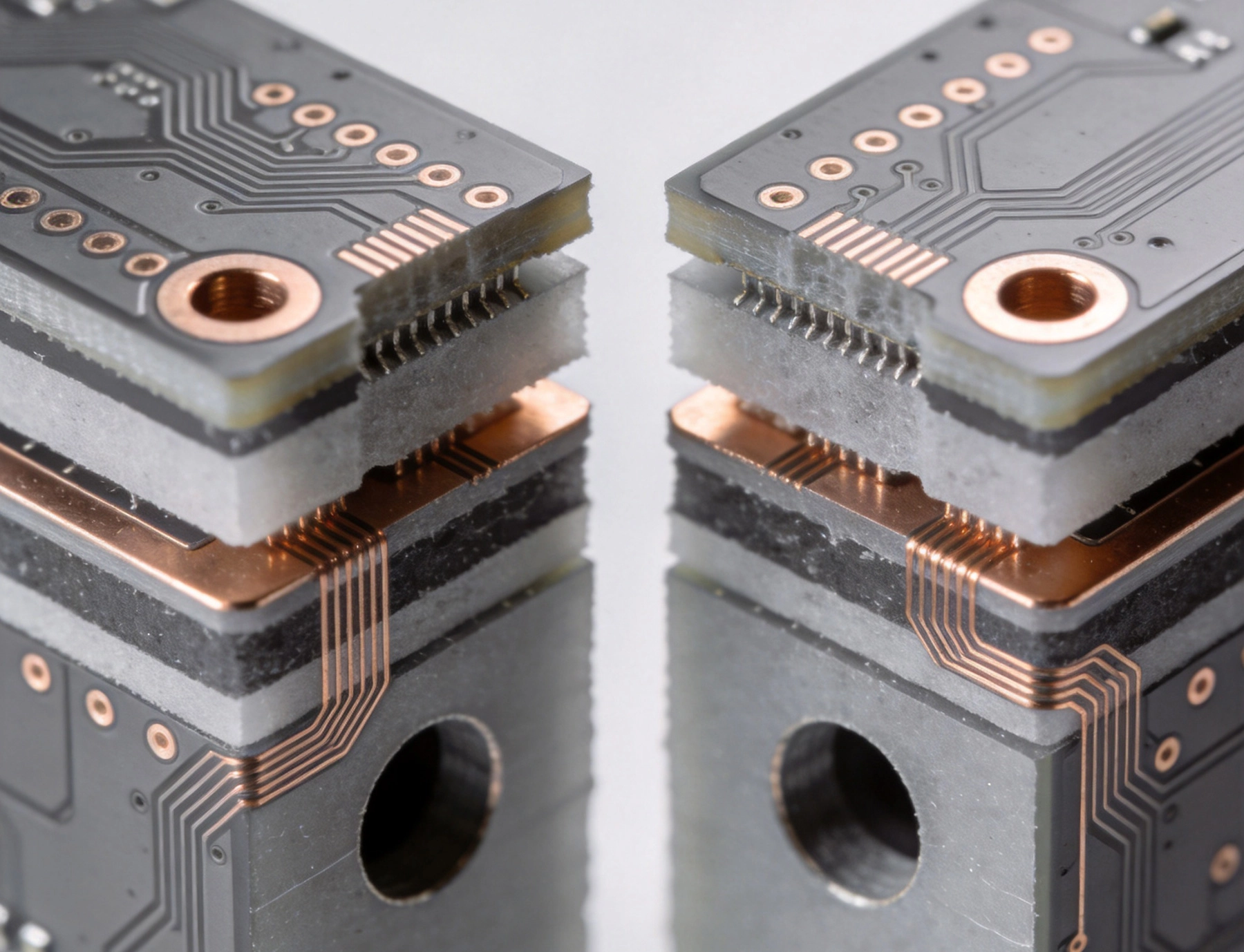
Through-hole vias have served as the backbone of Multilayer Pcb interconnects for decades. These cylindrical copper-plated holes extend through the entire board thickness, creating electrical connections between layers. The concept is straightforward: drill a hole through all layers, then plate the walls with copper to form a conductive pathway.
The primary advantage of through-holes lies in their reliability and established manufacturing processes. Every PCB fabricator can produce through-holes reliably, and the technology has been refined over decades of production experience. Through-holes also provide robust mechanical connections, making them ideal for applications requiring high reliability or where components will be mounted directly to the via pads.
However, through-holes consume significant board real estate. A standard 0.3mm through-hole via with appropriate annular rings requires a pad diameter around 0.6mm, plus routing channels for traces passing between vias. In dense designs, through-holes can occupy 15-20% of available board space, forcing larger board dimensions or additional layers to accommodate routing requirements.
Standard through-hole diameters range from 0.15mm to 0.35mm for typical multilayer designs, with aspect ratios (board thickness to hole diameter) typically limited to 10:1 or less. Higher aspect ratios create plating challenges and reliability concerns, particularly for boards exceeding 1.6mm thickness. Designers must balance hole size against plating reliability and current-carrying capacity requirements.
Through-holes also create design restrictions beyond simple space consumption. Because they pass through all layers, component placement on inner layers becomes constrained—you cannot place components beneath through-hole vias on inner layers. This limitation becomes increasingly significant as component densities increase and board sizes shrink.
Microvias represent a fundamentally different approach to layer interconnection. These small-diameter vias, typically 0.1mm or smaller, connect only adjacent layers rather than passing through the entire board. Laser Drilling enables precise formation of these microscopic structures, allowing significantly higher via densities than traditional mechanical drilling can achieve.
The space savings from microvias can be dramatic. A microvia pad might measure 0.25mm or smaller, compared to 0.6mm for through-holes. This reduction allows placing microvias directly in component pads, under components, or in routing channels where through-holes would be impossible. For High-density Interconnect designs, microvias enable routing patterns that would be physically impossible with Through-hole Technology alone.
Microvias are created using Laser Drilling rather than mechanical drill bits. The laser ablates the dielectric material precisely, creating a clean cavity that is then copper-plated to form the electrical connection. This process enables aspect ratios up to 1:1 for standard designs, compared to the 10:1 or less typical for through-holes. The tighter aspect ratio tolerance enables reliable microvias even in thin dielectric layers.
Several microvia configurations exist, each serving different design requirements. Blind Vias start from an outer layer and terminate at an inner layer, visible from one side of the board. Buried Vias connect inner layers only, invisible from either board surface. Stacked microvias place multiple vias vertically in the same location, connecting non-adjacent layers through sequential build-up processes.
Staggered microvia arrangements offer an alternative to stacking. Instead of placing vias directly above one another, staggered configurations offset each layer's via position slightly. This approach can simplify manufacturing and improve reliability by avoiding potential weak points at via intersections, though it consumes slightly more space than stacked configurations.
The choice between blind, buried, and stacked microvias depends on your specific routing requirements and layer stack-up. Complex HDI designs often combine multiple microvia types to optimize routing density while managing thermal and mechanical stress distribution across the board.
The decision between microvias and through-holes involves multiple tradeoffs across three critical dimensions: board space, manufacturing cost, and long-term reliability.
Microvias dramatically reduce via-related space consumption compared to through-holes. A typical through-hole via with pad occupies approximately 0.28 square millimeters of board space, while a microvia in-pad might use only 0.05 square millimeters. For designs requiring thousands of vias, this difference translates to significant board size reductions or fewer routing layers needed.
The space advantage becomes even more pronounced when considering via-in-pad designs. Microvias can be placed directly within component pads, eliminating the routing channels that through-holes require. This capability enables tighter component placement and shorter signal paths, improving electrical performance in addition to saving space.
Through-holes generally cost less to manufacture than microvias. Mechanical drilling uses proven processes available at virtually every PCB fabricator, while laser drilling microvias requires specialized equipment and expertise. The cost differential varies based on via density, with microvias becoming more economical relative to through-holes as via counts increase and board sizes decrease.
However, total system cost matters more than via cost alone. If microvias enable reducing board size from four layers to six layers, or shrinking board dimensions by 30%, the overall material and processing cost savings often outweigh the per-via premium. Designers should evaluate total board cost, not just via fabrication cost, when making technology decisions.
Through-holes offer proven reliability across decades of field deployment. The simple cylindrical structure provides robust electrical and mechanical performance, with well-understood failure modes and design guidelines. For applications where reliability is paramount—automotive, aerospace, medical implants—through-holes provide confidence backed by extensive field history.
Microvias have accumulated substantial reliability data themselves, particularly since their adoption in mobile devices and consumer electronics. However, stacked microvia configurations can create stress concentration points, and thermal cycling may cause different failure mechanisms than through-holes experience. Designers should work closely with fabricators to understand reliability testing data for specific microvia configurations under consideration.
Despite the space advantages of microvias, through-holes remain the optimal choice for many applications. Understanding when through-holes excel helps designers avoid over-engineering solutions with unnecessary complexity.
Choose through-holes for designs with moderate density requirements where board space isn't critically constrained. If your application can accommodate standard routing channels and doesn't require via-in-pad placement, through-holes offer simpler manufacturing and proven reliability without HDI complexity. Many industrial control boards, Power Electronics, and general-purpose applications fall into this category.
Applications requiring maximum reliability under harsh environmental conditions often benefit from Through-hole Technology. The robust mechanical structure handles thermal cycling, vibration, and mechanical stress effectively. For automotive under-hood electronics, aerospace systems, and medical devices where failure isn't an option, through-holes provide confidence backed by extensive field experience.
Cost-sensitive applications with moderate volume requirements typically favor through-holes. If your design doesn't require the density advantages of microvias, avoiding HDI processes reduces both tooling costs and per-unit manufacturing expenses. For prototypes and low-volume production, through-holes enable faster turnaround from a broader range of fabricators.
Microvias become essential when design requirements push beyond what through-hole technology can reasonably achieve. Several application categories benefit substantially from microvia implementation.
High-density designs requiring fine-pitch components—BGA packages with 0.4mm pitch or finer, chip-scale packages, or dense IC arrays—typically require microvias to escape signals from component pins. Through-holes simply cannot fit within the routing channels between fine-pitch pads. Mobile devices, tablets, and wearables exemplify applications where microvias enable physical designs that would be impossible with through-holes alone.
High-speed designs benefit from microvias' shorter electrical paths. Because microvias connect adjacent layers rather than traversing the entire board thickness, they present lower inductance and capacitance than through-holes. For signals operating at multi-gigahertz frequencies, this electrical advantage can be critical for maintaining Signal Integrity and timing margins.
Layer count reduction represents another microvia advantage. If a design would require eight layers with through-holes but only six with microvias, the layer count reduction may offset the microvia fabrication premium. Fewer layers mean less material cost, simpler stack-up, and potentially improved impedance control. Evaluate total board cost, not just via cost, when making this assessment.
Many successful designs combine microvias and through-holes, leveraging the advantages of each technology where appropriate. This hybrid approach optimizes both space utilization and cost efficiency.
Consider using microvias for signal escape routing from dense components, then transitioning to through-holes for general-purpose routing in less congested board areas. This approach provides the density advantage of microvias where needed without applying expensive HDI processing across the entire board surface.
Power distribution networks often benefit from through-holes' robust current-carrying capacity, while signal routing uses microvias for density. The larger copper cross-section of through-holes handles power delivery more effectively than microvias, making this a natural division of responsibility between the two technologies.
Ground and power planes typically use through-holes for stitching and thermal vias, where multiple vias work together rather than requiring minimal space. Signal routing layers employ microvias for escape routing and layer transitions, optimizing density where it matters most for routing complexity.
Successful implementation requires following established design guidelines for each technology while managing transitions between them effectively.
Standard through-hole designs follow proven guidelines: minimum hole diameter typically 0.15mm for mechanical drilling, annular ring requirements of 0.15mm or more depending on fabrication capabilities, and aspect ratios limited to 10:1 for reliable plating. Higher aspect ratios may be achievable with controlled drilling parameters but require careful coordination with fabricators.
Via spacing should maintain adequate clearance for routing channels between adjacent vias. A general guideline allows 0.3mm Minimum Trace Width between through-hole pads, though actual requirements depend on fabricator capabilities and design complexity. Consider routing requirements early in the design process, as through-hole placement density directly impacts routing channel capacity.
Microvia design rules differ significantly from through-holes due to different formation processes. Laser-drilled microvias can achieve diameters down to 0.05mm in some processes, though 0.1mm represents a practical production minimum for most fabricators. Aspect ratios should be limited to 1:1 for standard designs, with tighter ratios possible for thin dielectric materials.
Copper land diameter should provide adequate annular ring for reliable plating, typically 0.25mm total for 0.1mm microvias. Via-in-pad designs require filled and planarized microvias to avoid solder joint reliability issues. This additional processing step adds cost but enables significant density improvements for fine-pitch component mounting.
Stacked microvia arrangements require careful Thermal Management considerations. Each via layer creates potential stress concentration points, and thermal cycling may induce different failure modes than single-layer microvias experience. Coordinate with fabricators on stacked microvia reliability testing data appropriate for your application environment.
Choosing between microvias and through-holes requires balancing multiple factors: board space requirements, cost targets, reliability needs, and manufacturing capability. Through-holes excel in applications where proven reliability, moderate density, and cost efficiency matter most. Microvias become essential for high-density designs, fine-pitch components, and applications where board space savings justify additional manufacturing complexity.
Many successful designs combine both technologies strategically, applying microvias where density demands require them while using through-holes for power distribution and less space-constrained routing. This hybrid approach optimizes total system cost while achieving necessary performance targets.
Work closely with your PCB fabricator early in the design process to understand their capabilities and design guidelines for both technologies. Their input on cost tradeoffs, reliability data, and manufacturing constraints helps optimize your via technology selection for specific application requirements.
Microvias offer significantly higher density than through-holes, enabling via-in-pad placement and routing in spaces where through-holes cannot fit. A microvia might occupy 0.05 square millimeters compared to 0.28 square millimeters for a through-hole, enabling dramatic board size reductions or layer count decreases for dense designs.
Per-via cost is higher for microvias due to laser drilling requirements, but total board cost depends on how via technology affects overall design. If microvias enable reducing layers or board size, total cost may actually decrease despite higher per-via expense. Evaluate total system cost, not just via fabrication cost, when making technology decisions.
Through-holes typically offer higher current-carrying capacity than microvias due to larger copper cross-section. For power distribution networks requiring substantial current delivery, through-holes often prove more effective. However, parallel microvias can achieve similar current capacity while maintaining density advantages in signal routing areas.
Via-in-pad places microvias directly within component pads, enabling signal escape routing from fine-pitch components that would be impossible with through-holes. This technique requires filled and planarized microvias to prevent solder joint reliability issues. Use via-in-pad for BGA packages with 0.4mm pitch or finer, or where maximum routing density is essential.
Stacked microvias place vias directly above one another, maximizing space efficiency but creating potential reliability concerns at via intersections. Staggered microvias offset each layer's position slightly, improving reliability while consuming marginally more space. Choose stacked for maximum density requirements; choose staggered when reliability concerns outweigh space optimization needs.

Understanding HDI PCB Stack-ups: Best Practices for High-Density DesignsJuly/18/2026

How We Ensure Quality Control in Multilayer PCB LaminationAugust/08/2026
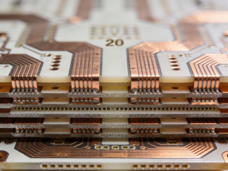
How to Design High-Layer Count PCBs (20+ Layers) for Complex ElectronicsSeptember/08/2026
Durability Requirements for Industrial IoT PCBs: Ensuring Reliability in Harsh EnvironmentsSeptember/03/2026
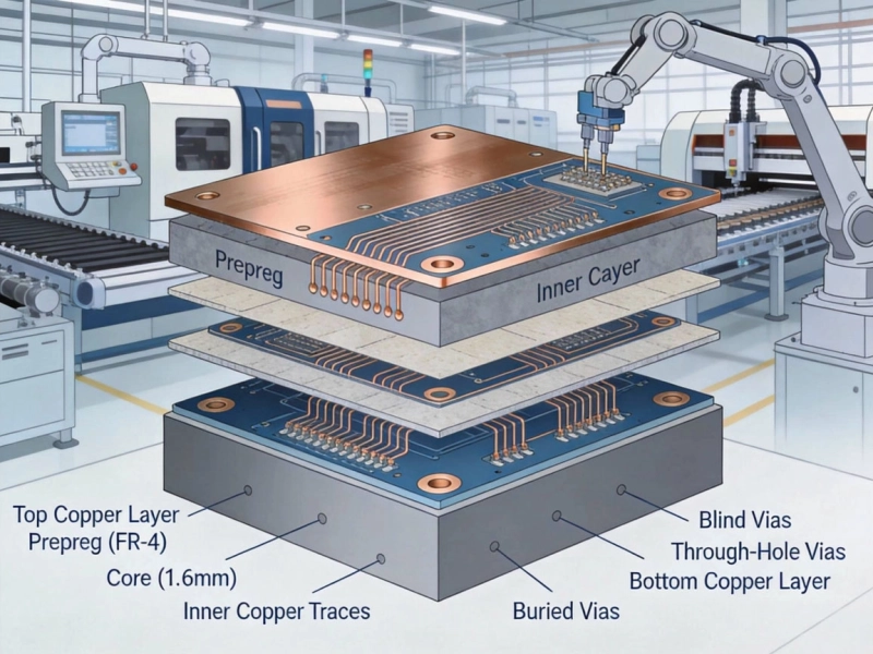
What Are Multilayer PCBs? A Complete Guide from ChinaMay/18/2026

Behind the Scenes: A Tour of Our State-of-the-Art PCB Factory in ChinaMay/19/2026

China vs. Local PCB Suppliers: Analyzing Cost, Quality, and Lead TimeJuly/22/2026

Metal Core PCBs in EV Charging Stations: Managing High HeatJuly/30/2026