
Every PCB project eventually faces the same fork in the road: thru-hole technology (THT) or Surface Mount Technology (SMT). It's not a trick question, but getting the answer wrong costs you in rework, reliability failures, or a bloated bill of materials. Engineers who've been in the industry for a while know that the "right" choice usually depends less on personal preference and more on the specific demands of the application, the production volume, and the operating environment.
This guide cuts through the noise. We'll walk through what each technology actually does, where they differ in ways that matter for your project, and how to make a decision that holds up when the board hits the field.
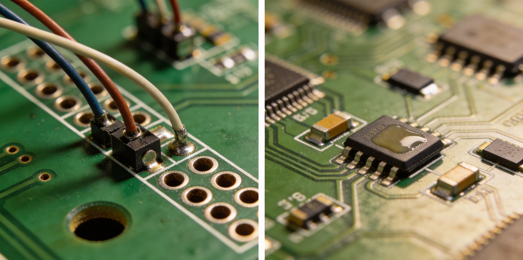
Thru-hole technology has been the backbone of Electronics Manufacturing since the 1950s. The process is straightforward: component leads are inserted into drilled holes on the PCB, and then the board passes through a wave soldering process that solders the leads on the opposite side. The result is a mechanical connection that's often stronger than the PCB substrate itself.
Tht Components come in several package types that you probably recognize: axial leads, radial leads, and DIP (dual in-line package) are the most common. Each lead passes completely through the board, creating a physical bond that resists vibration, thermal cycling, and mechanical stress far better than surface mount joints alone.
In our experience running Turnkey PCB Assembly projects, we still reach for thru-hole parts when the end application demands ruggedness above all else. Military and aerospace customers in particular frequently specify THT connectors and electromechanical components because those joints can take a beating without cracking.
Surface Mount Technology arrived in the 1980s and fundamentally changed how PCBs are built. Instead of inserting leads through holes, SMT components are placed directly onto the surface of the board, where solder paste holds them in place during the reflow oven. The component sits on pads rather than passing through the substrate.
The size difference is dramatic. A standard SOIC (small outline integrated circuit) package takes up a fraction of the board real estate of its through-hole DIP equivalent. When you scale that across an entire board with hundreds of components, SMT enables designs that would be physically impossible with thru-hole parts alone. Modern consumer electronics, from smartphones to laptops, rely entirely on SMT for this reason.
Smt Assembly also lends itself to automation in ways that thru-hole never could. Pick-and-place machines can mount dozens of components per second, and the reflow oven process is highly repeatable with minimal operator intervention. For high-volume production runs, that speed translates directly into lower per-unit costs.
If your board is going into an environment with significant vibration, mechanical shock, or repeated thermal cycling, the mechanical advantage of thru-hole becomes hard to ignore. The lead passing through the board creates what engineers call a "form fit" connection — the hole walls and the solder work together to resist pull-out forces. An SMT joint, by contrast, is essentially a surface adhesion problem. Under enough mechanical stress, the solder joint can crack.
We tested this on a recent industrial motor control project. The customer had originally designed everything in SMT for cost savings, but field returns showed a recurring solder joint failure pattern at the connector interface — exactly where cables get plugged and unplugged thousands of times. Switching those connectors to thru-hole eliminated the problem within two production cycles. The per-unit cost went up slightly, but the cost of field failure — returns, replacements, reputation damage — made the math obvious.
That said, SMT isn't fragile. Modern lead-free solder alloys and proper Dfm (Design For Manufacturing) practices produce joints that survive substantial stress. The key is matching the technology to the actual environment, not defaulting to one approach based on assumptions.
This is where SMT dominates without much contest. Surface mount components can be stacked on both sides of the board, placed in tight rows with minimal spacing, and routed underneath large IC packages using blind and Buried Vias. Thru-hole technology, by its nature, requires physical clearance around each hole for insertion and soldering, which limits how densely you can place parts.
For a product where Miniaturization is a core requirement — a wearable device, a compact sensor module, a drone controller — SMT is essentially the only viable path. Trying to achieve the same board density with thru-hole components would require a board roughly three times larger, which defeats the purpose of the entire design.
The trade-off is in the prototyping stage. SMT component placement demands either precision manual assembly (which is slow and error-prone for fine-pitch parts) or access to a pick-and-place machine. Thru-hole prototyping can be done with a basic soldering iron and a steady hand, which matters when you're iterating on a design in-house.
For high-volume runs — say, ten thousand units or more — SMT is the clear economic winner in most scenarios. Automated assembly is faster, more consistent, and requires less manual labor. A modern SMT line can populate a complex multi-layer board in minutes, while thru-hole assembly typically requires more operator involvement, especially for odd-shaped or oversized components.
However, for low-volume or prototype runs, the cost picture shifts. SMT setup costs — programming the pick-and-place machine, creating solder paste stencils, configuring the reflow oven profile — can make small batches disproportionately expensive on a per-unit basis. Thru-hole assembly, with its simpler tooling and the ability to use hand assembly for small quantities, often works out cheaper for prototype runs under fifty units.
This is one of the most common miscalculations we see in turnkey projects: engineers optimize their design for the production volume they expect in year three, but their first-order prototypes cost twice as much as they should because they didn't account for the assembly cost dynamics of low-volume runs.
Thru-hole leads provide a direct, low-inductance path through the board. For high-current applications, this can be a meaningful advantage — the mechanical connection is physically more substantial, and current can flow through the lead rather than relying solely on the surface pad and trace. In Power Electronics where thermal cycling is a concern, we've found thru-hole connections hold up better over extended periods.
SMT components, on the other hand, often offer better high-frequency performance because the lead inductance is lower (shorter connection length) and the package can be designed with Controlled Impedance in mind. Many RF and microwave designs exclusively use SMT for this reason. The smaller parasitic elements matter at high frequencies in ways they don't for power or digital logic applications.
Heat Dissipation is another consideration. Thru-hole components can be bolted directly to heatsinks or chassis elements through their leads, providing a thermal path that's harder to achieve with SMT. Conversely, SMT components on metal-backed PCBs can achieve excellent thermal performance through the substrate itself, especially when thermal vias are placed under power components.
Based on hundreds of Turnkey Assembly projects, the clearest indicators for choosing thru-hole are:
SMT is the right choice when:
In reality, most production boards use both technologies. The connectors are thru-hole for mechanical strength, the passive components are SMT for density, and the main ICs may be SMT for size and performance. A mixed-technology approach isn't a compromise — it's often the most engineering-appropriate solution.
Building a mixed-technology board requires careful process planning. The typical sequence is: SMT components on the top side go through reflow first. Then the board is flipped, and thru-hole components are inserted either manually or with an automatic insertion machine. Finally, the board goes through wave soldering to create the thru-hole joints, taking care that the previously soldered SMT joints on the top side aren't disturbed by the wave.
The challenge increases with lead-free solder requirements. Lead-free wave solder temperatures run higher than traditional tin-lead processes, which raises the risk of reflowing previously mounted SMT joints. Working with an assembly partner who understands mixed-technology process control — including proper reflow profiling and flux selection — makes a measurable difference in first-pass yield rates.
Regardless of which technology you lean toward, a few Dfm principles consistently show up in boards that assemble cleanly the first time:
There is no universal winner between thru-hole and SMT. The decision framework we use internally is straightforward: start with the constraints that are hardest to change — the operating environment, the size requirements, and the production volume. Those three factors narrow the choice faster than anything else. From there, look at the component-level requirements, and you'll usually find that a mixed-technology approach gives you the best balance of performance, cost, and manufacturability.
If you're working on a project where the assembly approach isn't yet locked in, walk through those questions with your design team before finalizing the layout. A board that needs to be redesigned because the wrong assembly technology was assumed at the start is one of the most avoidable cost overruns in Electronics Development.
For those already in the middle of a project with assembly questions, the right assembly partner can make a significant difference — not just in execution, but in guiding the design decisions that affect cost and quality long before the first board is populated.
Yes, and this is standard practice in most production electronics. Mixed-technology boards are assembled in a specific sequence — SMT first, then thru-hole insertion followed by wave soldering — to avoid damaging previously placed components. Working with an experienced assembly partner helps optimize the process for first-pass yield.
For high-volume production, SMT is generally less expensive per unit because it is fully automated. For low-volume or prototype runs, the setup costs of SMT can make thru-hole or manual assembly more economical. The exact crossover point depends on board complexity, component count, and the specific assembly partner's capabilities.
Thru-hole is generally preferred for components that need to withstand vibration, shock, and thermal cycling, which are common in industrial and outdoor applications. However, SMT boards designed with appropriate DFM practices and high-Tg materials can also perform well in demanding environments. The connector interfaces, regardless of board technology, are almost always specified as thru-hole for mechanical durability.
It depends on your density requirements. Thru-hole technology can be used in moderately dense designs, but you will hit a practical limit where the board area required for through holes becomes prohibitive. For ultra-compact designs, SMT is necessary. The solution many designers use is a hybrid approach: thru-hole for mechanical and high-current parts, SMT for everything else.
Yes, Smt Assembly requires a pick-and-place machine, a reflow oven, and a solder paste stencil, which represent a significant capital investment. However, for most projects, you don't need to own this equipment — working with an established assembly service provider gives you access to these capabilities without the capital outlay. The per-unit economics of SMT only improve when the volume is high enough to spread that equipment cost across many boards.
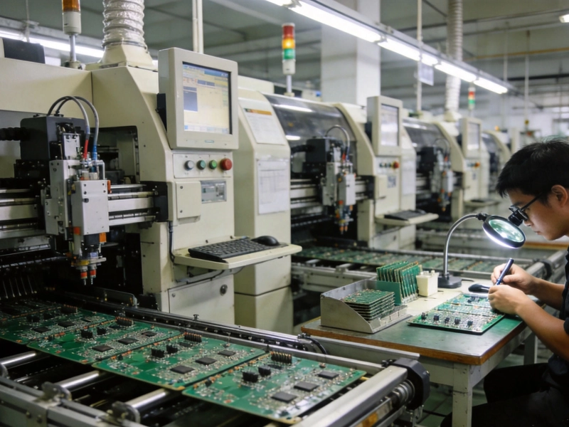
The Complete Guide to SMT PCB Assembly in ChinaJune/17/2026
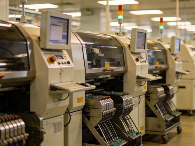
Turnkey PCB Assembly: Simplifying Your Supply Chain with One VendorOctober/10/2026
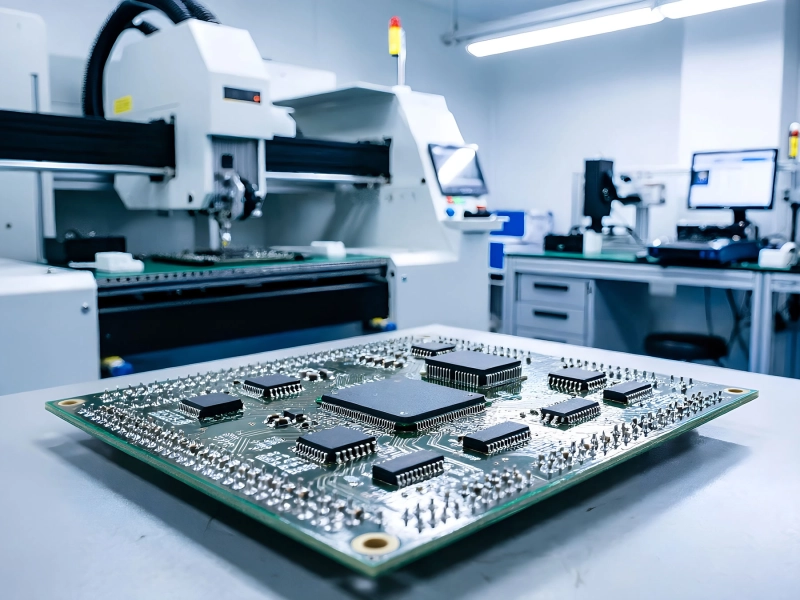
Top 10 DFM Mistakes to Avoid Before Sending Files to China for SMT AssemblyJuly/15/2026
Designing for SMT: Pad Sizes, Spacing, and OrientationJuly/12/2026
BGA Assembly Challenges: X-Ray Inspection and Voiding IssuesSeptember/17/2026
What to Look for in a Reliable SMT PCB Assembly Partner in ChinaAugust/10/2026
Emergency PCB Runs: Can Chinese Manufacturers Meet Tight Deadlines?August/14/2026
The Rise of Flexible PCBs in Foldable Phone HingesJuly/14/2026