Open Nav

Your high-speed Pcb Design is supposed to deliver clean, reliable signals at gigabit speeds. Instead, your oscilloscope shows ringing, overshoot, and ghosts that should not be there. The culprit is almost certainly signal reflection. Understanding why signal reflection happens in your High-speed Pcb is the first step toward fixing it and ensuring your design performs as intended.
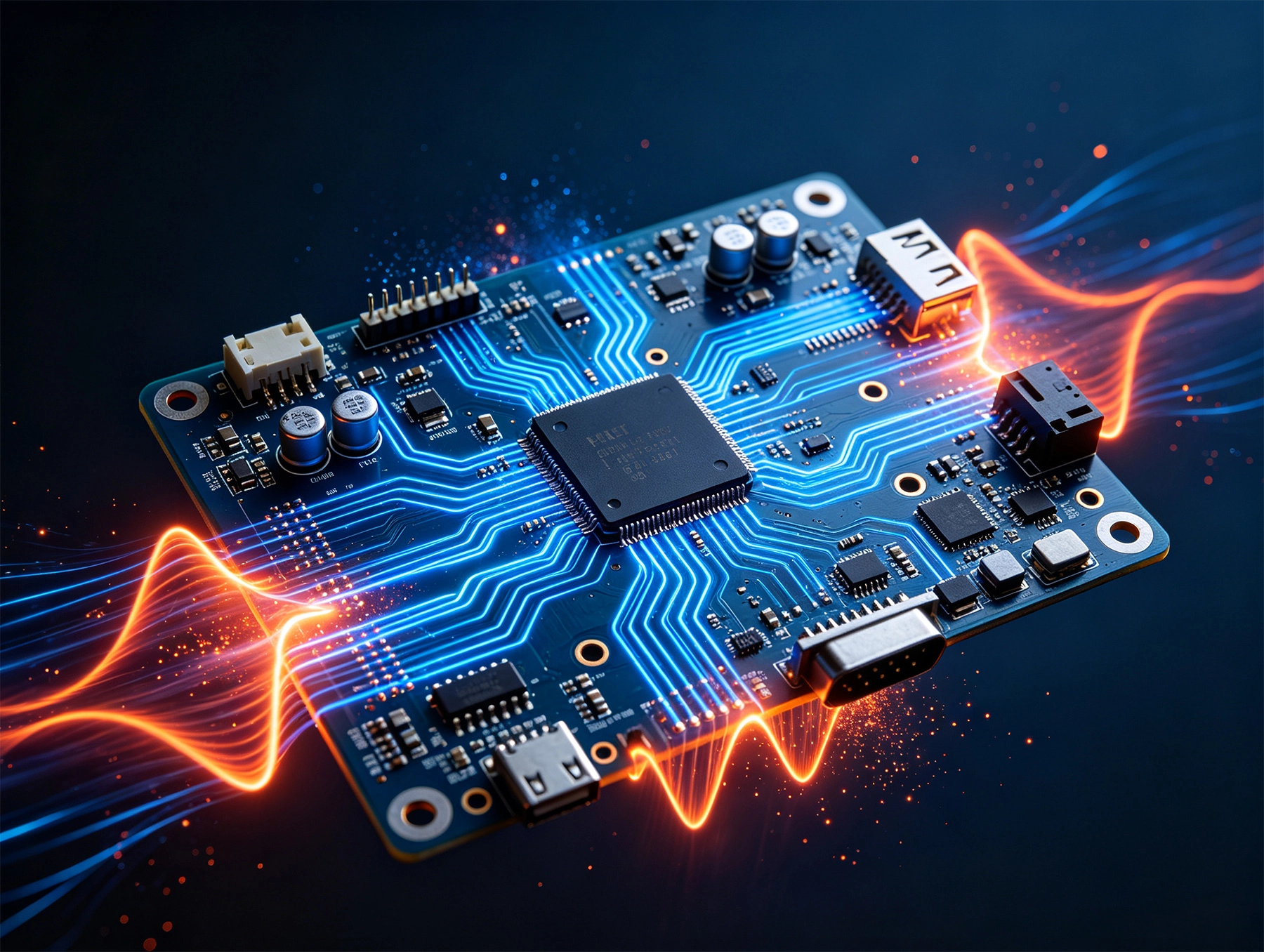
Signal reflection occurs when a traveling electromagnetic wave encounters a change in the electrical environment along its path. Think of it like a sound echo in a tunnel: the sound wave travels until it hits a boundary, then part of it bounces back toward the source.
In a PCB trace, the signal propagates along the transmission line from driver to receiver. When the trace geometry, layer stackup, or termination changes abruptly, the signal sees a different characteristic impedance than what it expected. Part of the signal energy reflects back toward the source, while the rest continues forward.
The reflected signal superimposes on the original, creating the ringing patterns you observe on your scope. At low speeds, these reflections settle before the receiver samples the signal. At high speeds, the data rate exceeds the reflection settling time, and the receiver interprets corrupted voltage levels, resulting in bit errors.
The fundamental cause of signal reflection is impedance mismatch. Every transmission line has a characteristic impedance determined by its geometry and the dielectric properties of the surrounding material. When the actual impedance encountered differs from the line impedance, reflection occurs.
The reflection coefficient determines how much of the signal reflects back. It equals (ZL - Z0) / (ZL + Z0), where ZL is the load impedance and Z0 is the line impedance. When ZL equals Z0, the coefficient is zero and no reflection occurs. The greater the mismatch, the larger the reflection.
Common impedance mismatches in High-speed Pcb designs include:
Low-speed PCB designs rarely experience significant signal reflection problems because the signal wavelength is much longer than the physical discontinuities. A 1 MHz signal has a wavelength of approximately 200 meters in FR4. Discontinuities measured in millimeters represent negligible fractions of the wavelength, so reflections have no measurable impact.
At high speeds, everything changes. A 5 Gbps signal has a rise time of roughly 50 picoseconds. In FR4 with a dielectric constant of 4.5, the signal wavelength during this transition is only about 8 millimeters. Discontinuities that are 1 millimeter or even fractions of a millimeter become significant compared to the wavelength.
When the physical length of a discontinuity approaches or exceeds one-quarter of the signal wavelength, it behaves as an electrical stub and causes resonance. This is why high-speed signals are far more sensitive to routing geometry, via design, and termination strategy.
Beyond simple impedance mismatches, high-speed PCB designs must account for several transmission line phenomena that do not matter at low frequencies.
At high frequencies, current flows primarily on the surface of conductors due to the skin effect. This reduces the effective cross-sectional area, increasing resistance and causing attenuation. While this does not directly cause reflection, it affects Signal Integrity by distorting pulse shapes and reducing noise margins.
PCB laminate materials absorb some signal energy, converting it to heat. The loss tangent of the dielectric material determines how significant this effect is. Low-loss materials like Rogers Rogers 4003 or Panasonic Megtron 6 exhibit less signal degradation than standard FR4 at high frequencies.
Different frequency components of a signal travel at slightly different speeds in the dielectric material. Over long distances, this spreads out the pulse edges and degrades signal quality. Dispersion becomes more pronounced with higher data rates and longer trace lengths.
Understanding typical design errors helps you avoid them in your own high-speed PCB layouts.
Failing to terminate transmission lines properly is the most common cause of signal reflection in high-speed designs. Many engineers remember to terminate differential pairs but forget about single-ended high-speed signals. Even when termination is present, using the wrong value destroys its effectiveness.
Series termination resistors work best near the driver for point-to-point routing. Parallel termination at the receiver end suits bidirectional signals. Thevenin termination provides termination through voltage divider biasing. Each approach has trade-offs, and choosing incorrectly for your application creates worse problems than no termination at all.
Through-hole vias with unused stubs act as open-ended transmission lines. The signal enters the via, reaches the stub bottom, and reflects back. For high-speed signals, these stubs resonate at frequencies determined by their electrical length, creating severe discontinuities.
Back-drilling removes the unused portion of through-hole vias. Blind and Buried Vias eliminate stubs entirely but increase manufacturing cost. Always consider via stubs when routing high-speed signals through boards with multiple layers.
The return current for a signal trace flows in the adjacent reference plane, directly beneath the signal trace for microstrip or between two planes for stripline. Any break, slot, or via antipad in the reference plane forces the return current to take a longer path, increasing loop inductance and creating impedance discontinuities.
Routing high-speed signals across board folds, connector cutouts, or around large mounting holes forces return current to navigate around obstacles. The resulting inductance spike creates reflection at the discontinuity point.
High-speed differential signals rely on close coupling between the two conductors. When the positive and negative traces have unequal lengths, the signal components arrive at the receiver at different times. This intra-pair skew reduces common-mode rejection and creates timing violations that manifest as reflection-like noise on the differential waveform.
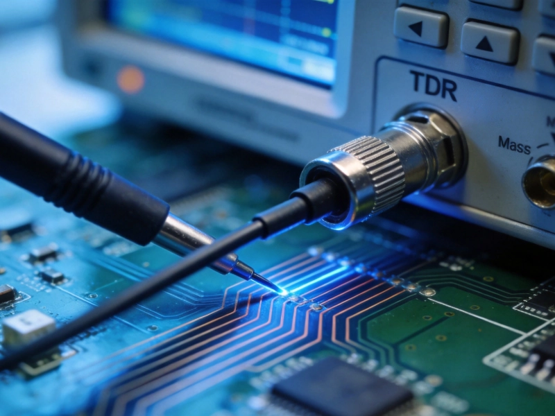
Identifying reflection sources in an existing design requires systematic measurement and analysis. Your oscilloscope time-domain reflectometry (TDR) capability provides the most direct insight into impedance discontinuities.
A TDR sends a fast rise-time pulse down the trace and displays the reflected waveform. Peaks in the TDR trace indicate locations where impedance is higher than nominal. Dips show where impedance is lower. The amplitude of the feature correlates with the magnitude of the mismatch.
Most modern high-bandwidth oscilloscopes include TDR functionality. You can also use a dedicated TDR instrument or a vector network analyzer with TDR capability for more detailed characterization.
For manufacturing troubleshooting, time-domain transmission (TDT) measurements show how signals are distorted as they propagate through the board. Comparing measured eye diagrams against expected results reveals cumulative Signal Integrity issues, including reflection effects.
Fixing signal reflection requires addressing both design and manufacturing factors that contribute to impedance discontinuities.
Select termination resistance to match the characteristic impedance of your transmission line. For 50-ohm single-ended traces, use 49.9-ohm or 51-ohm resistors rather than round numbers. Precision matters because even 5% tolerance creates measurable mismatch at high speeds.
Place series termination resistors as close to the driver output as possible. The goal is to absorb reflections from the receiver by dampening the oscillation before it propagates far. For receiver-end termination, ensure the resistor connects directly to the reference plane with minimal stub length.
Design your layer stackup for consistent Controlled Impedance. Work with your PCB manufacturer to define dielectric thickness, trace width, and copper weight tolerances that achieve your impedance targets within acceptable variation.
Maintain consistent trace geometry by avoiding fanouts that transition from wide to narrow traces. Use 45-degree angles rather than 90-degree corners. Keep high-speed trace widths constant from driver to receiver, even if this requires slightly longer routing.
Use blind and Buried Vias for high-speed signals when your design permits the additional manufacturing cost. When through-hole vias are necessary, specify back-drilling to remove unused stubs on critical nets.
When vias cannot be avoided, use via-in-pad technology with Microvias to minimize the impedance discontinuity. Include ground vias adjacent to signal vias to provide a controlled return path through the transition.
Never route high-speed signals over slots, gaps, or splits in the reference plane. If a split is unavoidable, use a stitching capacitor or bridge connection to maintain return current continuity across the boundary.
Avoid routing high-speed signals near board edges where the reference plane may be incomplete. Keep clearances from the board edge at least three times the trace width to minimize parasitic effects.
Use serpentine routing or adjustable meanders to match intra-pair lengths within your timing budget. For very high-speed differential signals, 1 mil of skew can matter. Account for different propagation velocities if the positive and negative signals travel on different layer types.
Your PCB substrate material significantly impacts high-speed signal transmission. Standard FR4 works adequately for speeds up to approximately 1-2 Gbps, but higher speeds benefit from low-loss materials specifically engineered for RF and high-speed digital applications.
Key material properties include:
For complex high-speed designs with multiple gigabit-per-second links, board-level simulation helps predict signal integrity issues before manufacturing. Electromagnetic simulation tools can model your entire signal path, including layer stackup, trace geometry, vias, and connectors.
Signal integrity simulation tools like Keysight ADS, Cadence Sigrity, and ANSYS HFSS provide insight into reflection behavior, crosstalk, and timing margins. Running simulations early in the design cycle, when layout changes are inexpensive, prevents costly respins caused by signal integrity failures.
Even with simulation, physical testing remains essential. Simulation models contain approximations, and manufacturing variations introduce real-world effects that simulation cannot capture. Budget time and resources for validation testing on prototype hardware.
Close collaboration with your PCB manufacturer improves the likelihood of achieving your signal integrity targets. Share your impedance requirements and critical net classifications during the design phase, not after layout is complete.
Request impedance test coupons on your production panels. These test structures, fabricated alongside your boards using identical processes, enable verification that the manufactured impedance matches your design intent. When coupons fail to meet targets, your production boards may also deviate.
Discuss via design options with your manufacturer. Some facilities offer controlled-depth drilling, Sequential Lamination, or other processes that minimize via discontinuities for high-speed applications. Understanding what is possible helps you make informed design trade-offs.
Signal reflection in high-speed PCBs results from impedance discontinuities that cause portions of the signal energy to reflect back toward the source. These reflections distort the signal waveform, reducing noise margins and potentially causing bit errors at high data rates.
The primary causes include impedance mismatches from missing or incorrect termination, via stubs, reference plane discontinuities, and routing geometry changes. High-speed designs are particularly vulnerable because the signal wavelength approaches the physical dimensions of these discontinuities.
Solutions focus on elimination: proper termination, Controlled Impedance design, via stub management, reference plane integrity, and careful differential pair length matching. Material selection also matters, with low-loss laminates providing cleaner signal transmission at multi-gigabit speeds.
Diagnosis uses TDR measurements to locate discontinuities, while simulation tools predict issues early in design. Close collaboration with your PCB manufacturer ensures that the fabricated board matches your signal integrity requirements.
By understanding why signal reflection occurs and applying systematic design practices, you can achieve reliable high-speed performance in your PCB designs.
If your high-speed signals show ringing, overshoot, or undershoot on oscilloscope measurements, or if you observe elevated bit error rates that correlate with specific traces or operating conditions, signal reflection is likely contributing to your problem. Use TDR measurements to confirm impedance discontinuities.
Match your termination to the characteristic impedance of your transmission line. For standard 50-ohm single-ended traces, use a 49.9-ohm or 51-ohm resistor. For 90-ohm differential pairs, use 88.7-ohm or 91.3-ohm resistors to account for coupling effects.
Sometimes yes. Adding external termination resistors near the driver or receiver may help. Reducing data rate or increasing signal margins can improve reliability even when reflection is present. However, fundamental geometric issues like via stubs or reference plane problems require board revision to fully resolve.
FR4 works for data rates up to approximately 1-2 Gbps with careful design. For higher speeds, low-loss materials like Rogers or Panasonic Megtron series provide better signal integrity. The choice depends on your specific data rate, distance, and reliability requirements.
Typical tolerance requirements are ±10% for general digital signals. High-speed signals with tight margins may require ±5% or better. Discuss your requirements with your manufacturer and specify tolerances accordingly in your design documentation.
Signal reflection is a fundamental challenge in high-speed Pcb Design, but it is entirely manageable with proper design practices, material selection, and manufacturing collaboration. Understanding the root causes and applying systematic solutions ensures your high-speed designs perform reliably.

Finding the Right China Flexible PCB Manufacturer for Wearable TechJune/12/2026

Metal Core PCBs in EV Charging Stations: Managing High HeatJuly/30/2026
ADAS Systems and the Need for High-Speed, High-Frequency PCBsSeptember/20/2026

Top 10 DFM Tips to Avoid Errors in Your Next PCB OrderJune/18/2026
Case Study: Solving a Complex Thermal Issue with a Metal Core PCBOctober/12/2026
Why Medical Devices Require Specialized High-Reliability PCB ManufacturersSeptember/15/2026

From Gerber to Delivery: How We Achieve 24-Hour PCB PrototypingJuly/09/2026
Controlled Impedance Testing: Ensuring Performance in High-Speed BoardsOctober/15/2026