
Quality Control is the backbone of successful Electronics Manufacturing. In the fast-paced world of Surface Mount Technology (SMT) assembly, even minor defects can lead to product failures, costly recalls, and damaged reputations. This is where Automated Optical Inspection (AOI) becomes a game-changer. By leveraging advanced imaging technology and intelligent algorithms, AOI systems detect defects at speeds and accuracies that human inspectors simply cannot match.
In this comprehensive guide, we'll explore how AOI technology works, what defects it catches, and why it has become an indispensable part of modern SMT production lines—particularly for manufacturers seeking reliable Pcb Assembly services in China.
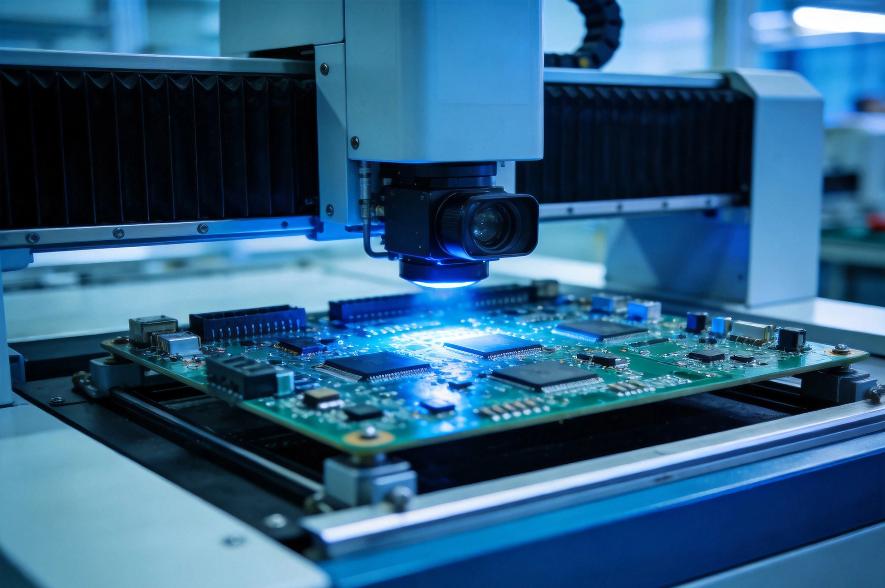
Automated Optical Inspection is a non-contact testing method that uses high-resolution cameras and sophisticated software to visually inspect printed circuit boards during and after the assembly process. Unlike manual inspection, which relies on human eyes and judgment, AOI systems capture detailed images of PCB surfaces and compare them against predefined standards or "golden samples."
The technology has evolved significantly since its introduction in the 1980s. Modern AOI machines feature:
These advancements make AOI systems particularly valuable for high-volume production environments where speed and consistency are paramount.
The first line of defense occurs before components are even placed. SPI-AOI systems examine solder paste deposits on PCB pads immediately after the stencil printing process. This early detection is critical because solder paste defects account for approximately 60-70% of all Smt Assembly issues.
SPI-AOI identifies problems such as:
Catching these issues before component placement prevents expensive rework and reduces material waste significantly.
After components are mounted but before reflow soldering, AOI systems verify proper component placement. This stage detects:
Early detection at this stage allows for quick rework before solder solidifies, saving both time and resources.
The final AOI checkpoint occurs after the reflow oven, where solder joints are formed. This is where the most comprehensive defect detection happens. Post-reflow AOI evaluates:
A single AOI machine can inspect hundreds of components per minute with consistent accuracy. Unlike human inspectors who experience fatigue and attention drift, AOI systems maintain the same detection performance throughout 24/7 operations. This speed advantage is crucial for high-volume production lines where throughput directly impacts profitability.
AOI eliminates subjective judgment from Quality Control. Each inspection follows programmed criteria, ensuring that the same standards apply to every board. This objectivity proves invaluable for:
The rule of thumb in Electronics Manufacturing is that defect detection cost increases tenfold at each subsequent production stage. Finding a problem during solder paste inspection costs pennies; discovering it after final assembly may require complete board replacement costing hundreds of dollars.
By implementing multiple AOI checkpoints, manufacturers:
Modern AOI systems do more than detect defects—they generate valuable data for process optimization. By analyzing defect patterns, engineers can identify root causes such as:
This data-driven approach enables predictive maintenance and continuous process refinement.
Traditional 2D AOI uses top-down cameras to capture planar images of PCB surfaces. These systems excel at detecting:
2D systems remain popular for cost-sensitive applications and boards with predominantly simple components.
Advanced 3D AOI employs multiple cameras or structured light projection to capture height information alongside traditional 2D images. This capability enables:
For high-reliability applications and dense PCB designs, 3D AOI has become the industry standard.
For boards with hidden solder joints—such as BGAs, QFNs, and other bottom-terminated components—AOI alone cannot inspect beneath the component body. Leading manufacturers combine AOI with Automated X-ray Inspection (AXI) to achieve complete coverage of all solder connections.
Effective AOI implementation requires careful positioning within the SMT workflow:
Each checkpoint serves a distinct purpose, and eliminating any stage reduces overall defect detection effectiveness.
AOI effectiveness depends heavily on proper programming. Key considerations include:
Investing time in thorough programming pays dividends through reduced false call rates and improved detection sensitivity.
Modern AOI systems integrate seamlessly with MES platforms, enabling:
This integration transforms AOI from a standalone inspection tool into a central component of Smart Manufacturing systems.
China's SMT industry has embraced AOI technology as a competitive differentiator. Leading Chinese Pcb Assembly facilities typically feature:
For overseas customers sourcing PCB assembly from China, verifying a manufacturer's AOI capabilities provides confidence in their quality commitment. Reputable facilities welcome questions about their inspection equipment, processes, and defect tracking methodologies.
While AOI is powerful, it has limitations. The technology cannot:
For comprehensive quality assurance, AOI works alongside:
A multi-layered inspection strategy combining these methods provides the highest confidence in product quality.
Automated Optical Inspection has transformed from a luxury technology to an essential component of modern SMT manufacturing. Its ability to detect defects at high speeds, with consistent accuracy, and at multiple production stages makes it invaluable for maintaining quality in today's demanding electronics market.
For companies sourcing PCB assembly services, understanding a manufacturer's AOI capabilities provides insight into their quality philosophy and operational sophistication. Facilities that invest in advanced AOI systems and integrate them into comprehensive Quality Management systems demonstrate commitment to delivering reliable, defect-free products.
As component sizes continue shrinking and PCB densities increase, the role of AOI in ensuring SMT quality will only grow more critical. Manufacturers who leverage this technology effectively gain significant competitive advantages through reduced costs, higher yields, and superior product reliability.
Ensure your next project benefits from comprehensive AOI inspection and industry-leading quality control. Contact our team to discuss your requirements and receive a detailed quotation for your PCB assembly needs.
2D AOI captures top-down images for planar inspection, while 3D AOI adds height measurement capabilities, enabling accurate solder joint volume analysis and coplanarity checking for fine-pitch components.
AOI detects most visible defects but cannot inspect hidden solder joints beneath components like BGAs. For complete coverage, AOI should be combined with X-Ray inspection and electrical testing.
Modern AOI systems inspect hundreds of components per minute, typically processing a standard PCB in 20-60 seconds depending on component density and inspection requirements.
While AOI provides maximum ROI in high-volume settings, it benefits low-volume production by ensuring first-article quality, reducing setup errors, and providing documentation for quality-sensitive applications.
Ipc-a-610 provides the industry-accepted criteria for solder joint quality and component placement, forming the basis for most AOI programming standards.
What is a Multilayer PCB? A Comprehensive Guide for EngineersJuly/02/2026
PCB Assembly Price China: A Complete Cost Guide for 2024May/18/2026
Thru-Hole vs. SMT: Choosing the Right Assembly Technology for Your PCBJuly/10/2026
How to Reduce Your PCB Manufacturing Costs Without Sacrificing QualityJuly/08/2026

Understanding PCB Assembly Prices in China: What Factors Influence Cost?June/10/2026
The Complete Step-by-Step Process ExplainedJune/05/2026
Cost-Benefit Analysis of Rigid-Flex PCBs vs. Traditional Cable AssembliesSeptember/14/2026
Preparing Your Gerber Files for a Smooth China PCB Fabrication ProcessSeptember/18/2026