Open Nav

Heavy copper for power. Fine pitch for intelligence. In an era where industrial controllers need to deliver tens of amps while running GHz-class processors on the same card, the question is not theoretical — it is a real design constraint that every PCB engineer eventually confronts.
Short answer: yes, you can mix heavy copper and Fine Pitch Components on one board. But "can" and "should" are very different conversations. The margin for error shrinks dramatically when you try to route 50A bus bars alongside 0.35mm pitch BGA packages on the same substrate. This article breaks down why it is possible, what makes it hard, and how to do it right the first time.
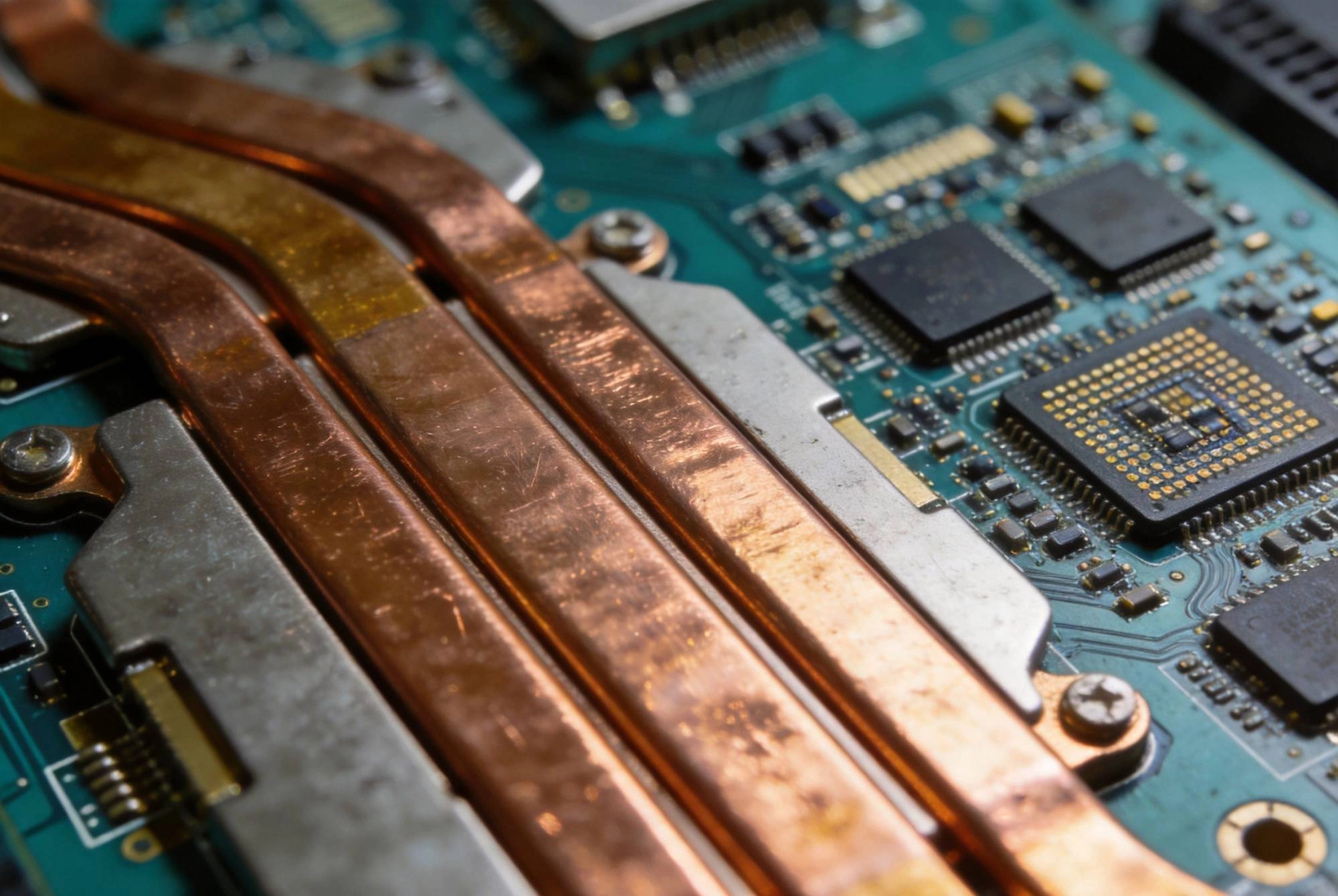
Modern industrial applications increasingly demand both high current and high density on a single PCB. A motor drive controller needs IGBT gate drivers (heavy copper, thick traces, large pads) alongside a microcontroller with DDR memory interface (0.4mm to 0.5mm pitch BGA or QFN). A power converter may need to host GaN FETs with ultrafine pad geometries alongside bus bars rated for 100A.
Keeping these functions on separate boards — one power board, one logic board — adds cost, connector overhead, and Signal Integrity penalties. Combining them into a single heterogeneous board saves space and eliminates inter-board interfaces. That is the prize. The challenge is that heavy copper and Fine Pitch Components have fundamentally different fabrication and assembly requirements.
The most serious problem is not electrical — it is mechanical. Heavy copper sections carry large currents and dissipate significant heat. Fine pitch components — particularly BGA and QFN packages — are extremely sensitive to temperature excursions during both assembly and operation.
When the coefficient of thermal expansion (CTE) of copper differs from the PCB laminate and the component package body, differential expansion creates shear stress at solder joints. A heavy copper region that heats up to 80°C or higher during operation sits just millimeters from a fine pitch device that should stay below 40°C for reliable lifetime operation. That thermal gradient across the board is the root cause of most mixed-technology board failures.
IPC-A-610 acceptance criteria for solder joint integrity under thermal cycling become much harder to meet when large copper features create non-uniform heating. Components near heavy copper planes experience steeper thermal gradients and higher cyclic strain.
Fine pitch components demand precise solder paste deposition, strict reflow profile control, and often nitrogen atmosphere reflow to prevent oxidation. Heavy copper pads, by contrast, act as heat sinks — they absorb a disproportionate share of reflow energy, cool faster, and can cause incomplete wetting on the component side of the joint.
Heavy copper pads are also more prone to solder wicking down plated through-holes, leaving insufficient fillet on the component side. This is especially problematic for fine pitch QFN packages where the exposed thermal pad relies on good solder flow to create a reliable thermal path and mechanical anchor.
Heavy copper areas — especially when reinforced with thick plating for high current — can exhibit surface height variations across the panel. These variations are invisible to the naked eye but large enough to cause non-contact issues during solder paste screening for 0.3mm-pitch components.
Surface finish selection also becomes more complex. Electroless Nickel Immersion Gold (Enig) is the standard choice for fine pitch assemblies because of its flat, uniform surface and excellent shelf life. However, heavy copper bus bars with Enig may develop excessive nickel corrosion under high current flow in humid environments. Immersion Silver or Osp on heavy copper sections may perform better for pure power delivery but offer less protection for fine pitch landing pads.
The most effective layout strategy is to physically separate heat-generating heavy copper regions from fine pitch component zones. Design a thermal keepout zone — typically 5mm to 10mm radius — around sensitive components where no high-current traces or planes are routed on adjacent layers directly beneath the component.
Use thermal relief spokes on heavy copper plane connections in these boundary zones to reduce conductive heat transfer into the fine pitch area. Full thermal connections (solid copper pour connections) are appropriate for power regions far from sensitive components, but thermal reliefs are essential at the thermal boundary.
A well-designed multilayer stack-up can actively route heat away from fine pitch areas. Place ground planes and power planes strategically so that heat from heavy copper regions spreads laterally and dissipates at the board edge rather than conducting vertically toward sensitive components.
For boards exceeding 3A per square centimeter in any zone, consider specifying high-Tg materials (TG 170 or higher) to raise the glass transition temperature and give the board more headroom against delamination under thermal stress. Materials rated to IPC-4101 slash 26 or slash 30 (high-Tg, CAF-resistant) are common choices for mixed-technology industrial boards.
Fine pitch QFN and BGA packages often have exposed thermal pads that must connect to the plane below. If that plane is heavy copper carrying high current, solder wicking becomes a serious risk.
The standard solution is to use via-in-thermal-pad with tented or plugged vias to prevent solder from draining away through the plated hole. For boards with heavy copper thermal planes, consider using a split thermal pad approach: a small thermal pad landing area under the component with heavy copper reached through thermal-relief spokes rather than direct fill. This reduces heat sink effect and controls solder flow during reflow.
Standard lead-free (SAC305) reflow profiles typically peak at 245°C to 260°C. When heavy copper is present, the soak zone should be extended by 30 to 60 seconds to allow the board surface to reach thermal equilibrium before the ramp to peak. This prevents cold solder joints on fine pitch pads that appear to wet but have marginal intermetallic formation.
For boards where heavy copper and fine pitch sections are on opposite sides, a double-sided assembly sequence is strongly preferred — populate and reflow one side, then the other. This avoids the situation where heavy copper pads on the bottom side create uneven heating that distorts the board during the second reflow pass.
When heavy copper traces must pass near fine pitch regions, use via stitching to distribute current across multiple smaller vias rather than relying on a single large copper feature. This reduces localized heating. Via stitching also adds mechanical reinforcement to the board, which helps the board resist flex during thermal cycling.
For layers carrying heavy current, specify copper weight explicitly in your fab drawing (e.g., 3oz outer layer, 2oz inner layers for power planes). Standard PCB Fabrication assumes 1oz copper as default — failing to specify the heavy copper requirement is one of the most common reasons boards come back from the fab with insufficient current-carrying capacity.
Before releasing your Design For Manufacturing, run through this checklist:
Have you defined a thermal separation zone around all fine pitch components? Specify the minimum distance from any heavy copper trace or plane edge to the nearest fine pitch pad. 5mm minimum is a practical starting point for boards with significant current density.
Have you specified heavy copper requirements explicitly in your fab drawing? Include copper weight per layer, and identify which sections of the board require heavy plating. Use callsouts on your fabrication drawing — do not rely on a notes field or verbal communication.
Are all thermal vias under QFN and BGA thermal pads tented or plugged? Specify tented on the component side, plugged on the solder side, or filled depending on your thermal requirements. Unmanaged via-in-thermal-pad is a leading cause of assembly defects in mixed-technology designs.
Have you reviewed your surface finish selection for compatibility with both power and fine pitch sections? ENIG is the most common choice but discuss any heavy copper areas with your manufacturer — large ENIG pads under high current may show signs of nickel corrosion over time in fielded products.
Has your Dfm review included thermal simulation or at least qualitative thermal analysis? Even a basic IR drop and heat flow simulation will reveal whether your power plane layout dumps heat into sensitive zones.
Have you confirmed your assembly house has experience with mixed-technology boards? Not all CM facilities have the reflow profile tuning capability and inspection equipment (X-ray for BGA, thermal imaging for high-current testing) required to reliably assemble and test boards in this category.
For boards where heavy copper sections carry sustained currents above 40A, or where fine pitch components are 0.3mm pitch or finer, seriously consider a two-board architecture — a power board and a logic/control board connected through press-fit connectors or soldered board-to-board connectors.
The mechanical and thermal complexity of merging these two extremes onto one substrate often exceeds the cost and space savings. A modular architecture gives each board its own optimized stack-up, surface finish, and assembly process. The added connector cost is frequently less than the engineering and test cost of debugging a marginal single-board design that fails field quality targets.
That said, for moderate current levels (10A to 30A) and 0.4mm pitch or coarser fine pitch devices, a single mixed-technology board is entirely achievable with good design practices. Many industrial motor drives, power supplies, and energy storage controllers are built this way successfully.
Boards with up to 4oz copper on outer layers and 3oz on inner layers can be combined with 0.4mm pitch BGA and QFN components. Beyond 4oz, the heat sink effect during reflow and the mechanical stress under thermal cycling make reliable fine pitch assembly increasingly difficult. Consult your assembly partner early — fabricators and CMs have different capabilities at the heavy copper end of the spectrum.
Osp (Organic Solderability Preservative) works well for fine pitch pads because it is flat and wettable. However, OSP degrades rapidly on heavy copper pads in high-humidity environments and offers no corrosion resistance for exposed bus bars. If your board has heavy copper areas that will be handled or exposed in service, ENIG or Immersion Silver are more appropriate overall finishes.
Solder wicking is controlled by managing the thermal mass difference between the component pad and the through-hole barrel. Key measures: tent or plug vias in thermal pads, use thermal relief connections rather than direct fill connections for component thermal pads, and specify appropriate solder paste volume for thermal pad land areas. Discuss via management with your CM during Dfm review — this is an area where CM-specific process knowledge makes a significant difference.
Yes, indirectly. Heavy copper regions that generate heat create non-uniform temperature distribution across the board during thermal cycling. BGA solder joints located near heat sources experience higher cyclic strain ranges than those in cooler zones. The fatigue life of joints near heavy copper regions can be 30% to 50% shorter than joints in thermally neutral zones for the same cycling condition. Thermal separation zones and high-Tg materials mitigate this significantly.
ENIG (Electroless Nickel Immersion Gold) is the most common choice for mixed-technology boards because it provides a flat, uniform surface for fine pitch landing pads and reasonable corrosion resistance for heavy copper sections. For boards with very high current density on heavy copper areas, discuss selective ENIG (applied only to fine pitch zones) or hybrid finish approaches with your manufacturer. Immersion Silver is an alternative for boards where cost is a primary driver and the operating environment is controlled.
Mixing heavy copper and fine pitch components on one board is not only possible — it is standard practice in industrial motor drives, power converters, and smart energy systems. The technical challenges are real: thermal mismatch between heat-generating copper and temperature-sensitive packages, solder wicking on heavy copper thermal pads, assembly process conflicts, and surface finish trade-offs. But these challenges are all solvable with good upfront planning.
Define your thermal zones, specify your copper weights explicitly, manage thermal pad via structures carefully, and engage your assembly partner during Dfm Review. For designs above 40A or with 0.3mm pitch or finer components, a two-board modular architecture may be the more cost-effective choice — but for the majority of industrial applications in the 10A to 30A range with 0.4mm or coarser fine pitch devices, a single mixed-technology board assembled by an experienced manufacturer will deliver reliable performance.
Contact us to discuss your requirements.
Need It Fast? The Benefits of a Quick Turn PCB Manufacturer in ChinaJune/16/2026

How AI is Transforming PCB Design and Manufacturing EfficiencyJuly/16/2026
How to Verify the Quality of a PCB Prototype Before Mass ProductionOctober/13/2026

PCB Fabrication China: A Complete Guide for Global BuyersMay/18/2026

Understanding PCB Assembly Prices in China: What Factors Influence Cost?June/10/2026
Evaluating a China Multilayer PCB Manufacturer: Certifications and CapabilitiesSeptember/11/2026
Microvias vs. Through-Holes: Choosing the Right Tech for Your Multilayer BoardAugust/06/2026

Why Automotive Electronics Demand High-Reliability Multilayer PCBsJuly/13/2026