Open Nav

Jumping straight from design files to full-scale production is one of the most expensive mistakes a hardware team can make. A single undetected defect—say, a misaligned drill or a latent short—multiplies across thousands of boards, draining budget and schedule alike. That is exactly why verifying your Pcb Prototype before Mass Production is non-negotiable. This guide walks through the practical, step-by-step methods engineers use to confirm that a prototype meets every specification, so the production line runs without surprises.
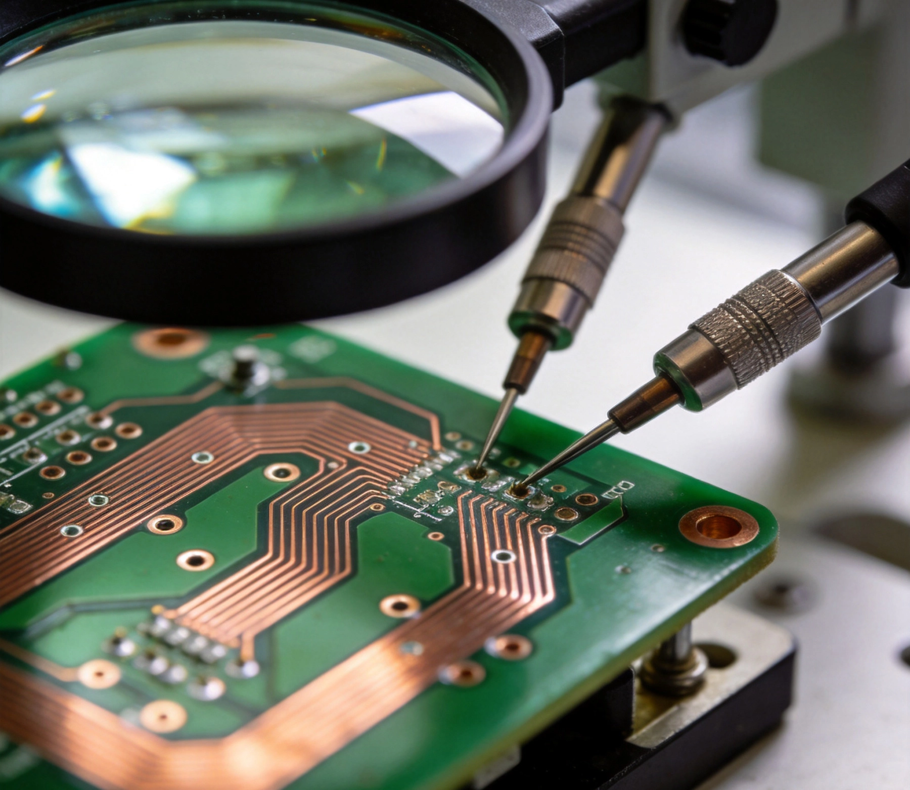
Mass Production amplifies everything. A solder mask opening that is 0.05 mm too small on one board becomes 5,000 rework jobs on a full run. A trace-width deviation that barely matters at low current can cause thermal failure on every single unit under real load. Prototype verification is the gatekeeper that catches these issues while the cost of correction is still measured in hours, not weeks.
Beyond catching defects, verification validates your design intent. Perhaps the impedance targets looked achievable in simulation, but the fabricated stack-up drifts enough to degrade signal margins. Or the via-in-pad structure you chose causes tombstoning on specific component pitches. The prototype is the first physical truth-check your design ever gets—treat it with the rigor it deserves.
The first line of defense is your own eyes—augmented with the right tools. Visual inspection catches a surprising range of issues: missing solder mask between pads, silkscreen over component land patterns, board outline routing errors, and obvious surface blemishes like scratches or contamination.
Use digital calipers or a coordinate measuring machine (CMM) to verify critical dimensions: board outline, mounting hole positions, connector cutouts, and keep-out zone clearances. Compare measured values against your Gerber files with tolerances applied. Any deviation beyond the specified tolerance—especially on features that mate with enclosures or connectors—needs resolution before you approve production.
For high-density designs, consider Automated Optical Inspection (Aoi) on the prototype. Aoi systems compare the fabricated board against the original design data and flag discrepancies in trace width, spacing, and pad geometry that human inspection misses, especially on dense BGA breakouts.
Visual inspection tells you the board looks right. Electrical testing tells you it is right. Two complementary methods cover the essentials: flying-probe testing and bed-of-nails (fixture-based) testing.
Flying-probe systems use moving test heads to contact nets individually, checking for opens and shorts without a custom fixture. This makes them ideal for prototypes—low setup cost, fast turnaround, and no permanent tooling investment. The trade-off is speed: each board takes minutes rather than seconds, which is fine for a prototype run but impractical at volume.
Ask your fabricator for a netlist comparison report alongside the flying-probe results. This cross-references every tested net against your original netlist, confirming that no nets were dropped, merged, or misrouted during fabrication.
If your prototype includes a test fixture—or if you are prototyping on a design that will use fixture-based testing in production—run the same test on the prototype. This validates not just the board but also the test coverage itself. Discovering that your fixture cannot access a critical net is a problem you want to find now, not on day one of production.
For high-speed designs, Controlled Impedance is a pass/fail parameter. Use a time-domain reflectometer (TDR) to measure the characteristic impedance of critical traces—typically differential pairs for USB, HDMI, or PCIe, and single-ended clock lines. Compare measured values against your stack-up specification. A deviation of more than ±10% from the target impedance generally warrants investigation, and tighter tolerances (±5% or better) are common for multi-gigabit interfaces.
Some quality attributes are invisible from the surface. Copper plating thickness in vias, interlayer registration accuracy, and laminate cure quality all live inside the board. A microsection—also called a cross-section—reveals these internal characteristics.
The fabricator cuts a small sample from the board (typically from a coupon area or the board edge), encapsulates it in epoxy, polishes the cross-section surface, and examines it under a microscope. Standard measurements include:
Request a microsection report with photographed images, not just numerical summaries. The images let you verify that the measurement points are representative and that no borderline conditions were averaged away.
Many fabricators perform microsections on test coupons rather than the actual board. Coupons are useful for process monitoring, but if your design has unusual via structures, heavy copper inner layers, or non-standard stack-ups, ask for a cross-section of the production board itself. The coupon may not capture the real plating distribution in a via-in-pad or a stacked micro-via.
A board that passes every dimensional and electrical check can still fail in assembly if the surface finish does not solder reliably. Solderability problems—caused by contamination, oxidized finishes, or expired shelf life—do not show up until components are placed.
For a prototype, you do not need formal IPC solderability test equipment. Instead, run a small wetting test:
If you see dewetting, non-wetting, or excessive solder ball formation, the surface finish may be contaminated or degraded. This is critical to catch early, because a finish problem affects every board in the production run until the root cause is corrected at the fab.
Different finishes have different shelf-life and handling sensitivities. Hasl (hot air solder leveling) is robust but uneven—fine-pitch pads may have thickness variation that affects stencil gasketing. Enig (electroless nickel immersion gold) provides a flat, solderable surface but can suffer from "black pad" nickel corrosion if the plating process is not tightly controlled. Osp (organic solderability preservative) is economical but has a short shelf life and is sensitive to handling. Know the failure modes of your chosen finish and inspect for them specifically.
You likely ran a Dfm check before ordering the prototype—but that was on paper (or rather, on Gerber data). Now you have the physical result. Use it to validate your Dfm assumptions.
If you find discrepancies, work with your fabricator to understand whether they are within their process capability or whether the design needs adjustment. Some issues are one-time fab errors; others indicate a systematic capability limit that will recur at volume.
For many applications, a prototype that works on the bench is not sufficient. You need confidence that it will survive its operating environment for its intended lifetime. Reliability testing provides that confidence.
Thermal cycling exposes mismatches in coefficient of thermal expansion (CTE) between the laminate, copper, and components. Run the prototype through accelerated thermal cycles—commonly -40 °C to +125 °C for industrial applications, or 0 °C to +100 °C for commercial. Monitor for via barrel cracking, delamination, and solder joint degradation. Even 50–100 cycles can reveal latent weaknesses that would emerge in the field over months or years.
IPC-TM-650 defines the solder float test: floating a board sample on a solder pot at 288 °C for 10 seconds, then inspecting for delamination or blistering. This is a quick, severe thermal shock test that catches lamination bonding problems. If your fabricator does not include this as a standard process qualification, request it on your prototype lot.
If the end product operates in humid environments, consider a moisture resistance test per IPC-TM-650 method 3.11. Expose the board to elevated temperature and humidity (typically 85 °C / 85% RH for 168 hours), then inspect for measling, blistering, or insulation resistance degradation. This is especially important for high-voltage designs where moisture ingress can cause catastrophic insulation failure.
Electrical continuity and impedance checks confirm the board is built correctly. Functional validation confirms it works correctly—and that distinction matters. A board with every net connected can still fail functionally if the stack-up impedance drifts enough to break a high-speed link, or if copper distribution causes warpage that prevents an IC from seating flat.
Populate the prototype with production-intent components and test it in a configuration as close to the final product as possible. Apply real power supply voltages, real signal loads, and real thermal conditions. Edge-case behavior—like a regulator oscillating under specific load transients, or a high-speed link dropping packets at temperature extremes—only surfaces under realistic operating conditions.
A single prototype passing functional test is encouraging but not conclusive. Build at least 3–5 units from the same lot, and if possible, from different production panels. Variability between units—whether in solder mask thickness, plating quality, or dimensional accuracy—tells you more about process stability than any single board can. If all five units pass identically, you have a much stronger basis for approving mass production than if one passes and four are marginal.
Verification without documentation is just opinion. Compile a formal prototype verification report that includes:
Each section should have a clear pass/fail verdict and a sign-off from the responsible engineer. This report becomes your quality baseline for production—it defines what "good" looks like, and it gives your production team a reference to compare against when first articles arrive from the mass production run.
Simulation is essential for design, but it assumes perfect materials and processes. The prototype is your first reality check. If measured impedance, thermal behavior, or signal quality diverges from simulation, believe the measurement. Investigate the gap, update your models if needed, and re-verify.
It is tempting to assume that because you ran DFM software before ordering, the fabricated board is automatically DFM-compliant. Fabrication processes have tolerances and occasional errors. Measure the real board and compare.
A good fabricator will flag concerns during production—tight spacings that pushed their capability, non-standard stack-ups that required special handling, or design features that reduced yield. Do not dismiss this feedback. It is a preview of the problems you will face at volume, where reduced yield directly impacts cost and lead time.
One passing prototype proves that it is possible to build a good board. It does not prove that the process consistently produces good boards. Always test multiple units from the prototype run.
Verifying a Pcb Prototype before mass production is a systematic process that spans visual inspection, electrical testing, cross-section analysis, solderability assessment, DFM validation, reliability stress testing, and functional evaluation under real conditions. Each step catches a different class of defect, and together they provide the confidence needed to commit to a production run with thousands—or hundreds of thousands—of boards.
The cost of thorough prototype verification is a fraction of the cost of a production failure. A bad prototype caught in verification costs you a revision cycle. A bad prototype released to production costs you a recall, a schedule slip, and a credibility hit. Verify first, then produce—it is the cheapest insurance you will ever buy for your hardware project.
Contact us to discuss your requirements for PCB prototype fabrication and verification support.
ISO and UL Certifications: What They Mean for Your PCB QualitySeptember/26/2026

How HDI PCBs Enable Slimmer Smartphones and TabletsJune/26/2026

Sourcing Metal Core PCBs for Automotive LED HeadlightsJuly/25/2026
How to Specify Bend Radius for Flexible PCB OrderAugust/06/2026

Supply Chain Resilience: Why Diversifying with a China PCB Partner HelpsSeptember/04/2026
ISO and UL Certifications: What They Mean for Your PCB QualitySeptember/23/2026
Dynamic vs. Static Flex: Which FPC Type Fits Your Project?July/20/2026
HDI PCB vs Standard PCB: Key Differences ExplainedMay/13/2026