Open Nav

Advanced Driver Assistance Systems, better known as ADAS, have moved from luxury-car novelty to mainstream expectation in less than a decade. Lane-keeping assist, adaptive cruise control, automatic emergency braking, and 360° surround-view are now standard trim items on mid-range vehicles. Behind every one of those features sits a stack of radar, lidar, camera, and ultrasonic sensors—and every one of those sensors demands a Printed Circuit Board that can move gigabits of data per second without flinching. That is why high-speed, high-frequency PCBs are no longer a niche specialty but a hard requirement for Automotive Electronics engineers.
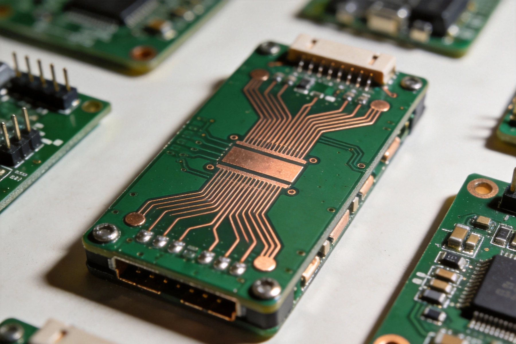
An ADAS-enabled vehicle is essentially a rolling data center. A single mid-range sedan may carry six radar modules (front long-range, front corner, rear corner ×2, side ×2), four to eight cameras, and a forward lidar unit. Each sensor streams raw or semi-processed data to a central compute platform—often called the Domain Controller or Zonal Controller—at rates from hundreds of megabits to several gigabits per second. The PCBs connecting these components must satisfy three simultaneous constraints:
Meeting all three on the same board—sometimes on the same layer—is what makes ADAS Pcb Design fundamentally harder than conventional Automotive Electronics.
Standard FR-4 (Dk ≈ 4.5, Df ≈ 0.02) is adequate for power distribution and low-speed CAN/LIN buses, but it fails spectacularly above roughly 2 GHz. At 77 GHz, the insertion loss through 10 mm of FR-4 microstrip exceeds 3 dB—enough to cut your received power in half before the signal even leaves the board. ADAS radar modules therefore use specialized high-frequency laminates:
A common stack-up strategy is the hybrid laminate approach: high-frequency material on the outer layers where RF traces and antennas live, and FR-4 or low-loss epoxy on inner layers for power and ground planes. This balances electrical performance against material cost, which matters when you are building millions of boards per year.
The PCB stack-up is the single most consequential design decision in an ADAS board. A well-designed stack-up simultaneously provides:
A typical 8-layer ADAS domain-controller stack-up might look like:
Notice that every signal layer has an immediately adjacent ground plane. That is not optional at 77 GHz; it is the difference between a board that works and a board that radiates.
A domain controller may route 12+ differential pairs from camera and radar inputs onto a single PCB region. Adjacent pairs separated by only 4–5 mils of dielectric will couple energy, especially when the signal edges are sub-50-ps. Mitigation requires:
Automotive PCBs endure thousands of thermal cycles between −40 °C and +125 °C over their 15-year service life. Dk and Dk stability matters because a 5 % drift in Dk at 77 GHz shifts the antenna beam and detunes the matching network. High-frequency laminates with ceramic PTFE cores (RO3003, RT/duroid 5880) offer Dk stability of ±0.04 across the automotive temperature range—far better than FR-4's ±0.2 drift.
ADAS boards sit inside metal housings attached to the vehicle chassis, but the housings have connector cutouts, vent holes, and harness grommets that act as slot antennas. At GHz frequencies, even a 6 mm slot is an efficient radiator. Board-level shielding cans, via fences along board edges, and meticulous return-path planning are mandatory to pass CISPR 25 Class 5 radiated-emission limits.
Designing a great stack-up is only half the battle. Fabricating it repeatably in volume is where many projects stumble.
First-article inspection should include time-domain reflectometry (TDR) on impedance test coupons, insertion-loss measurement on RF trace pairs, and cross-section verification of dielectric thickness on every layer pair.
ADAS PCBs face reliability stresses that consumer electronics never see:
Working with a PCB manufacturer who understands AEC-Q200 qualification requirements and offers PPAP (Production Part Approval Process) documentation is non-negotiable for Tier-1 automotive suppliers.
As the industry moves from Level 2 driver assistance toward Level 3 conditional automation and Level 4 high automation, the data throughput requirements escalate dramatically:
The PCB industry is responding with new materials and processes: embedded component technology (passives buried in inner layers to free surface area), Any-layer Hdi via structures for dense interconnect, and glass-ceramic hybrid laminates that push usable frequency beyond 110 GHz for next-generation imaging radar.
Not every PCB fabricator can build an ADAS board. When evaluating potential partners, ask specifically about:
A fabricator who can meet these criteria is not just a vendor—they are a design partner who will catch material-compatibility issues, stack-up risks, and manufacturability problems before they become expensive engineering changes.
ADAS is redefining what a "standard" Automotive Pcb looks like. The combination of multi-gigabit digital interfaces, 77 GHz millimeter-wave RF front-ends, and 15-year automotive reliability requirements creates a design space where material selection, stack-up architecture, impedance control, and manufacturing precision must all come together perfectly. There is no margin for "good enough"—a 2 % impedance error that would be invisible in a consumer gadget can take a radar module below its minimum detection range.
Engineers who treat ADAS Pcb Design as just another automotive board will learn, expensively, that it is not. The ones who invest in high-frequency materials, disciplined stack-up design, and a fabrication partner with proven automotive RF experience will deliver systems that see clearly, decide reliably, and keep drivers safe for the life of the vehicle.
If your team is developing an ADAS platform and needs a PCB manufacturer who understands the intersection of high-speed digital, millimeter-wave RF, and automotive reliability, contact us to discuss your stack-up, material, and manufacturing requirements.
FR-4's dielectric loss (Df ≈ 0.02) causes excessive signal attenuation above ~2 GHz. At 77 GHz, insertion loss through FR-4 microstrip is high enough to cripple radar range. High-frequency laminates with Df below 0.004 are required.
A hybrid stack-up combines high-frequency material (such as Rogers RO3003) on outer layers where RF traces live, with standard FR-4 or low-loss epoxy on inner layers for power and ground. This optimizes electrical performance while controlling material cost.
Most ADAS domain controllers use 6–10 layers. Radar sensor modules with integrated antennas often use 4–6 layers. The exact count depends on the number of high-speed differential pairs, RF trace density, and power-domain complexity.
Very-low-profile (VLP) or rolled-annealed copper is strongly recommended. Standard electrodeposited copper has surface roughness that adds 0.5–1.0 dB/in. insertion loss at 77 GHz compared to smooth copper.
Yes. Solder mask is lossy at millimeter-wave frequencies. Most 77 GHz radar designs specify solder mask openings over all RF traces and antenna structures to minimize dielectric loss and prevent Dk shift.

Metal Core PCBs in EV Charging Stations: Managing High HeatJuly/30/2026

Top 10 DFM Tips to Avoid Errors in Your Next PCB OrderJune/18/2026

Finding the Right China Flexible PCB Manufacturer for Wearable TechJune/12/2026

Why is My High-Speed PCB Experiencing Signal Reflection?September/07/2026
The Ultimate Guide to HDI PCB Technology You Need to KnowJune/02/2026

Speeding Up Product Development with Fast PCB Prototype ServicesJuly/27/2026

PCB Assembly Price China: A Complete Cost Guide for 2024May/18/2026

The Rise of Flexible PCBs in Foldable Phone HingesJuly/14/2026