Open Nav

As digital signaling speeds push past 10 Gbps and edge rates shrink to sub-nanosecond transitions, every fraction of an ohm matters. A PCB trace that deviates from its target impedance by even 5% can cause signal reflections, bit errors, and system-level failures that are notoriously difficult to debug. Controlled Impedance testing is the verification step that stands between a design that looks correct on screen and one that actually performs in the real world. This article walks through why impedance testing is non-negotiable for high-speed boards, how it is performed, and what it takes to consistently hit tight tolerances in production.
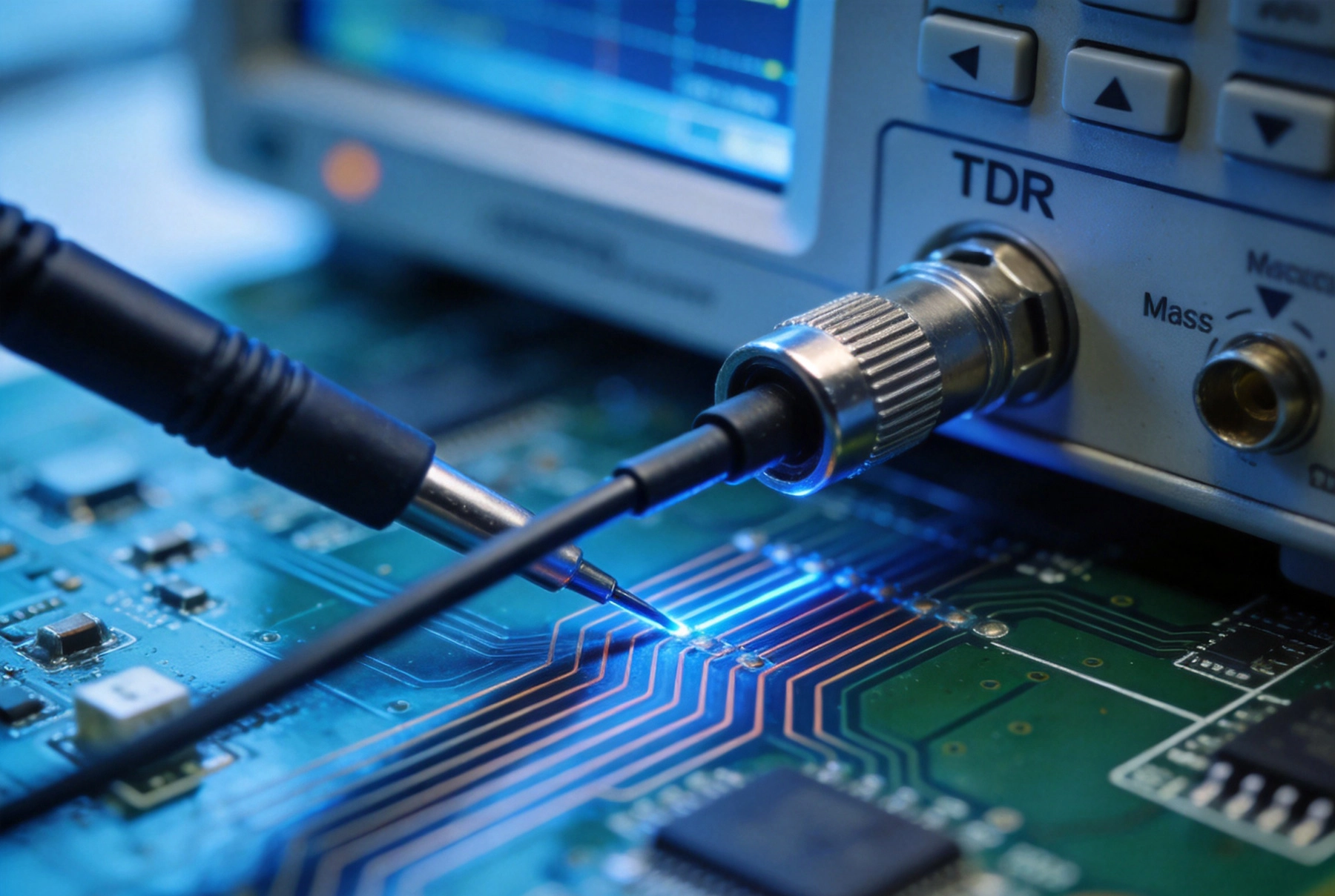
Impedance is not a property that you can see or touch on a finished board. It emerges from the interaction between trace geometry, dielectric properties, and the stack-up structure. When a high-speed signal encounters an impedance discontinuity—whether at a connector, a via transition, or a trace whose width drifted during etching—some of the signal energy reflects back toward the source. These reflections distort the signal waveform, increase jitter, and can push eye diagrams below acceptable mask boundaries.
Standards such as PCIe Gen5, USB4, and 400GBASE-KR4 specify impedance targets with tolerances as tight as ±5% or even ±3%. A 100-ohm differential pair that measures 93 ohms is out of spec and may cause interoperability problems with compliant transceivers. The only way to know for certain is to measure.
For a microstrip trace, characteristic impedance depends on trace width, trace thickness, dielectric constant (Dk) of the substrate, and the height of the dielectric layer between the trace and the reference plane. Stripline impedance adds the influence of the dielectric above the trace. The relationship is inverse: wider traces produce lower impedance, while thinner traces or thicker dielectrics produce higher impedance.
This means that anything which alters these physical dimensions during fabrication—copper plating variation, etch undercut, dielectric thickness changes during lamination, or Dk variation across a panel—directly impacts impedance. A well-designed stack-up targets a specific impedance value, but manufacturing tolerances will always introduce some deviation. Controlled Impedance testing quantifies that deviation.
Time-domain reflectometry (TDR) is the industry-standard method for measuring impedance on PCB traces. A TDR instrument sends a fast-rising step pulse down the trace and monitors the reflections that return. Since the amplitude and polarity of each reflection directly correspond to the local impedance at that point along the trace, the TDR builds a profile of impedance versus distance.
Key aspects of TDR testing include:
For differential impedance, a two-port TDR or a TDR with a differential probe pair is used. The instrument launches complementary signals on the two lines of the pair and measures the differential impedance directly, which accounts for any coupling between the traces.
Measuring impedance on actual circuit traces requires probing fine-pitch nets, which is time-consuming and risks damaging the board. Instead, PCB manufacturers include impedance test coupons on the production panel. These are dedicated traces that mirror the stack-up geometry of the target impedance nets but are placed in accessible areas with large probe pads.
An effective test coupon must satisfy several requirements:
When a design specifies controlled impedance, the fabricator adds these coupons automatically. The number and type of coupons depend on how many unique impedance structures exist in the design. A board with 50-ohm single-ended and 100-ohm differential pairs on multiple layers needs separate coupons for each combination.
Impedance tolerance defines the acceptable range around the target value. Common specifications include ±10% for general high-speed designs, ±7% for demanding applications, and ±5% or tighter for cutting-edge interfaces.
Several factors influence whether a manufacturer can meet a given tolerance:
A manufacturer's impedance capability statement should specify the tightest tolerance they can guarantee for each impedance value and layer count. This is not a marketing claim—it should be backed by statistical process control (SPC) data from production runs.
In a typical production flow, controlled impedance testing happens after lamination and before drilling or routing. The test coupons are accessible at this stage, and the impedance values reflect the final stack-up conditions. The process follows these steps:
Automated test systems can measure dozens of coupons in under a minute, making impedance testing a fast step even for panels with many unique impedance structures.
When impedance measurements fall outside tolerance, the root cause is typically one of the following:
Identifying the root cause quickly is essential because it determines the corrective action—whether that is adjusting the artwork, changing the lamination recipe, or switching to a different material grade.
Impedance control begins with the stack-up. A well-designed stack-up satisfies multiple goals simultaneously: target impedance on all layers, signal-to-reference-plane coupling for Signal Integrity, power delivery, and manufacturability. For impedance specifically, the designer must:
The stack-up should be developed in collaboration with the fabricator, who can validate that the proposed layer arrangement is producible and suggest adjustments to improve impedance yield.
While TDR is the workhorse of impedance testing, additional methods provide complementary information:
For most production applications, TDR coupon testing is sufficient. Advanced methods are reserved for design validation, material qualification, or debugging field failures.
IPC-2141 provides guidelines for controlled impedance design, while IPC-6012 and related standards address the workmanship requirements for finished boards. Although IPC does not prescribe a specific impedance tolerance for every application, it establishes the framework for documenting impedance requirements, test methods, and acceptance criteria.
For military and aerospace applications governed by MIL-PRF-31032 or similar specifications, impedance requirements are typically more stringent, and the test documentation must meet additional traceability standards. Medical device manufacturers subject to Iso 13485 also require detailed impedance test records as part of their Quality Management system.
Not every PCB fabricator can deliver tight impedance tolerances consistently. When evaluating potential manufacturing partners, consider the following:
A manufacturer who treats impedance as a core competency—not just an afterthought—will have the process controls, equipment, and expertise to hit your targets reliably.
To maximize the chances that your board passes impedance testing on the first run, keep these guidelines in mind:
Controlled impedance testing is the quality gate that verifies a High-speed Pcb will perform as designed. Without it, impedance targets are merely theoretical—hopeful predictions that may or may not survive the realities of Copper Etching, lamination pressure, and material variation. TDR-based coupon testing provides a fast, reliable, and non-destructive way to confirm that every production panel meets its impedance specifications.
For engineers working on modern high-speed interfaces, the message is clear: impedance testing is not optional. It is a fundamental part of the Manufacturing Process that directly determines whether your board will function at speed or fail silently in the field. Partnering with a manufacturer who has proven impedance capability, investing time in stack-up design, and specifying clear impedance requirements are the three pillars of success for any High-speed Pcb project.
Contact us to discuss your requirements for controlled impedance PCBs and learn how our manufacturing capabilities can support your high-speed designs.

High-Frequency PCBs in Radar and Satellite Communication SystemsAugust/03/2026
Smart Home Devices: Integrating High-Frequency PCBs for Wi-Fi/BluetoothSeptember/21/2026
Common DFM Mistakes in Rigid-Flex PCB Layouts: A Comprehensive GuideJuly/29/2026

Selecting a High-Speed PCB Manufacturer for 5G TelecommunicationsAugust/13/2026

Why Automotive Electronics Demand High-Reliability Multilayer PCBsJuly/13/2026
Why Medical Devices Require Specialized High-Reliability PCB ManufacturersSeptember/15/2026

What to Look for in a Reliable SMT PCB Assembly Partner in ChinaAugust/11/2026
The Ultimate Guide to HDI PCB Technology You Need to KnowJune/02/2026