
The smart home market has exploded in recent years, with devices ranging from voice-controlled speakers to automated thermostats becoming household essentials. Behind every seamless wireless experience lies a critical component that often goes unnoticed: the high-frequency Printed Circuit Board (PCB). These specialized PCBs enable reliable Wi-Fi and Bluetooth connectivity that consumers expect from their connected devices. Understanding how manufacturers integrate high-frequency PCBs into smart home products is essential for engineers and product designers working in this competitive space.
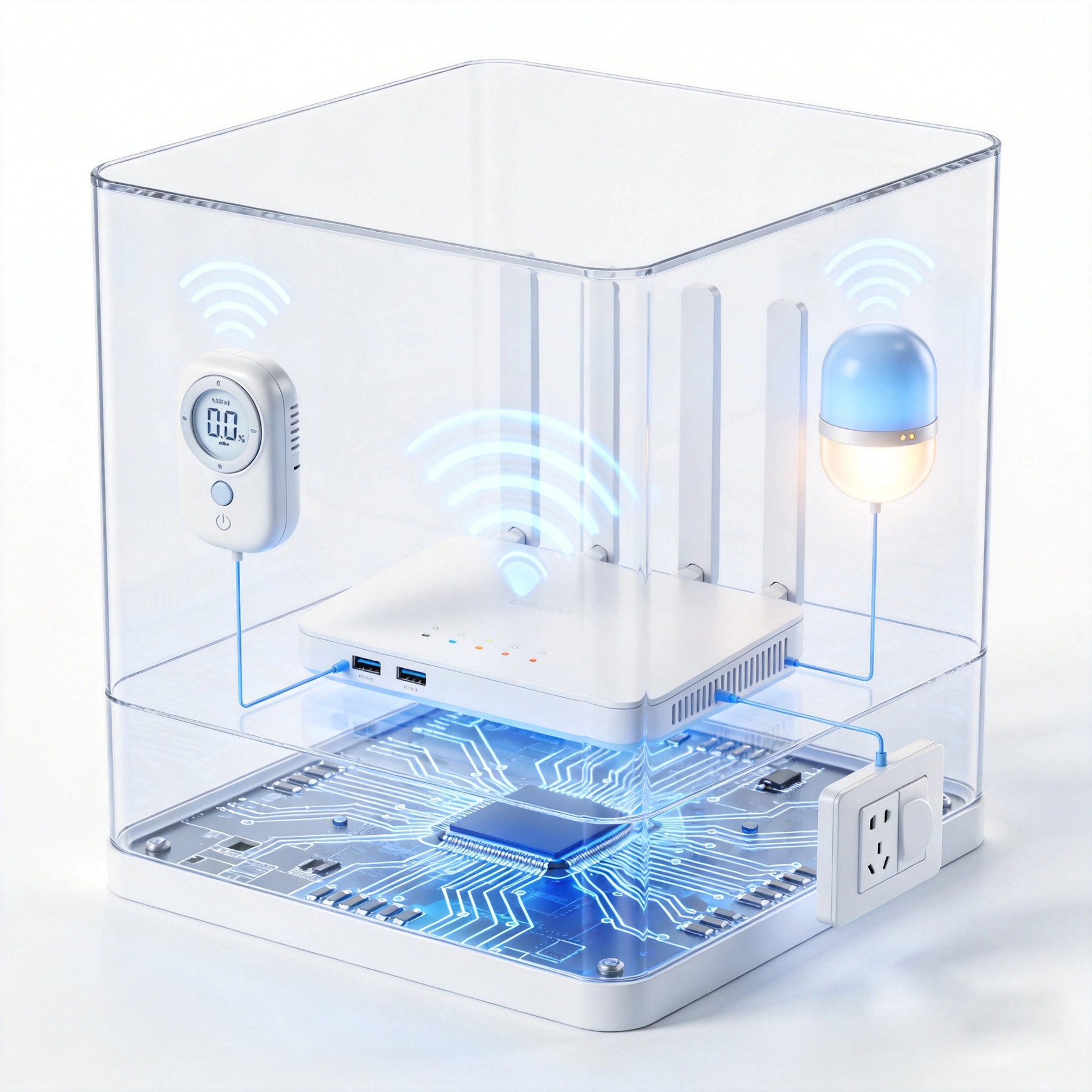
Smart home devices operate at frequencies that demand precision engineering. Wi-Fi networks commonly use 2.4 GHz and 5 GHz bands, while Bluetooth typically operates at 2.4 GHz as well. At these frequencies, traditional PCB materials can introduce signal loss, impedance mismatches, and electromagnetic interference that degrades performance. High-frequency PCBs solve these challenges by using specialized dielectric materials that maintain consistent electrical properties across the operating frequency range.
The difference becomes immediately apparent when examining real-world performance. A smart thermostat with a properly designed High-frequency Pcb maintains stable connectivity even in homes with thick walls or multiple floors. The same device built with standard materials might suffer from intermittent connectivity that frustrates users and leads to negative reviews. Manufacturers who invest in quality high-frequency PCBs deliver products that work reliably in challenging environments.
Selecting the right PCB material is one of the most consequential decisions in smart home device design. The two primary metrics that engineers evaluate are dielectric constant (Dk) and dissipation factor (Df). Materials with stable Dk values across temperature fluctuations ensure consistent impedance matching throughout the device lifecycle. Low dissipation factor materials minimize signal attenuation, which is crucial for battery-powered devices where every milliwatt matters.
FR-4 remains the most common PCB material due to its cost-effectiveness, but it falls short for demanding wireless applications. Rogers RO4003C and similar ceramic-filled hydro-carbon materials offer superior performance at frequencies up to 20 GHz. For Bluetooth applications where cost constraints are tighter, Panasonic Megtron 6 provides an excellent balance of electrical performance and manufacturing efficiency. Some manufacturers also use hybrid stackups that combine standard FR-4 layers with high-frequency materials in critical signal areas.
Smart home devices often experience wide temperature ranges. A smart lock installed outside must function reliably in both summer heat and winter cold. High-frequency Pcb materials must maintain stable dielectric properties across this temperature spectrum. Materials with low thermal coefficient of dielectric constant (TCDk) ensure that impedance matching remains consistent regardless of environmental conditions. This stability translates directly to reliable wireless performance for the end user.
The dissipation factor, often called loss tangent, measures how much signal energy converts to heat during transmission. At 2.4 GHz, standard FR-4 exhibits loss tangent values around 0.02, while high-performance materials like Rogers RO4350B achieve values below 0.004. This five-fold improvement in signal efficiency means more energy reaches the antenna, resulting in better range and lower power consumption. For battery-powered smart home sensors that must operate for years on a single battery, this efficiency gain directly impacts product viability.
Modern smart home devices frequently combine multiple wireless protocols in a single product. A smart speaker might support Wi-Fi for streaming, Bluetooth for quick pairing, and sometimes Zigbee or Z-Wave for home automation compatibility. This multi-protocol requirement complicates Pcb Stack-up Design significantly. Engineers must balance RF performance against manufacturing complexity and cost constraints.
Four-layer to six-layer stack-ups are typical for smart home devices. The outer layers typically host critical RF traces and components, while inner layers provide power distribution and ground planes. Maintaining a solid ground plane beneath RF traces is essential for controlling impedance and shielding against external interference. The spacing between signal layers and ground planes directly affects coupling and crosstalk characteristics.
High-frequency PCBs for Wi-Fi applications require precise Controlled Impedance traces. Wi-Fi signals typically use 50-ohm characteristic impedance for transmission lines. Variations beyond plus or minus ten percent can cause significant Signal Reflection and reduced throughput. Modern PCB manufacturers achieve impedance tolerances of five percent or better through careful trace width control and dielectric thickness management.
Microstrip and stripline configurations are the two primary options for Controlled Impedance routing. Microstrip traces on the outer layers offer easier manufacturing but are more susceptible to external interference. Stripline traces buried between ground planes provide superior shielding but require more complex manufacturing processes. Most smart home devices use a hybrid approach, with critical Wi-Fi and Bluetooth traces routed as striplines and antenna feed lines using controlled-impedance microstrips.
Vias present a significant challenge in high-frequency Pcb Design. They introduce inductance and capacitance that can disrupt Signal Integrity if not properly managed. For Wi-Fi applications operating at 5 GHz and above, via stub effects become particularly problematic. Back-drilling or blind/Buried Vias eliminate these stubs and maintain signal quality through layer transitions.
Grounded vias placed strategically around RF signal paths create shielding that reduces crosstalk between wireless circuits and digital processing sections. This technique, called via stitching, forms an electromagnetic cage that contains RF energy within the intended signal path. Proper via stitching is especially important in smart home devices where multiple wireless circuits must coexist without mutual interference.
The antenna represents the most critical element in any wireless system. Smart home devices typically use one of three antenna types: chip antennas, printed inverted-F antennas (PIFA), or external dipole antennas. Each option presents trade-offs between size, cost, and performance that engineers must navigate carefully.
Modern smart home devices increasingly favor integrated PIFA designs that conform to device geometry. These antennas utilize the PCB ground plane as part of the radiating structure, eliminating the need for separate antenna components. The PCB designer must carefully plan ground plane geometry and clearance areas around the antenna to achieve optimal radiation patterns.
Connecting the antenna to the RF transceiver requires a carefully designed matching network. This network, typically consisting of discrete inductors and capacitors, compensates for variations between the theoretical antenna design and actual manufactured conditions. Production tolerance variations can shift antenna impedance significantly, making precise component selection and tuning essential.
Many manufacturers use pi-network or T-network topologies for antenna matching. The pi-network offers superior harmonic rejection, which helps devices meet regulatory emission requirements. Network components must be placed as close to the antenna feed point as possible to minimize parasitic effects from trace inductance and capacitance.
Smart home devices often pack significant processing power into compact enclosures. Processors, wireless modules, and power management circuits all generate heat that must be dissipated effectively. High-frequency Pcb Design must balance thermal requirements against the need for dedicated RF sections with controlled impedance and minimal interference.
Thermal vias conduct heat from power components to ground planes or external heat sinks. These vias work in conjunction with thermal pads on component packages to provide efficient heat spreading. Some smart home devices incorporate metal core PCBs (MCPCBs) in areas with high thermal loads, combining the benefits of standard high-frequency materials for RF sections with superior thermal conductivity where needed.
Transitioning from prototype to high-volume production introduces additional complexity for high-frequency PCBs. Material lot-to-lot variations, Copper Thickness tolerances, and lamination consistency all affect final electrical performance. Manufacturers must establish tight process controls to ensure that production units match prototype performance specifications.
Quality verification typically involves time-domain reflectometry (TDR) testing to verify trace impedance and network analyzer measurements for S-parameter characterization. Flying probe testing checks for opens and shorts, while Aoi inspection verifies solder joint quality. High-frequency PCB manufacturers often provide impedance test coupons on each production panel to verify process consistency.
Volume production creates pressure to reduce costs without sacrificing wireless performance. Strategic material selection can achieve meaningful savings. For example, Isola I-Tera MT400A offers RF performance approaching Rogers materials at a significantly lower price point. Similarly, Rogers Ultralam 3850HT enables lower-cost Flexible Circuit solutions for smart home applications requiring bend-to-fit installation.
Design Optimization also contributes to Cost Reduction. Minimizing layer count where possible reduces material and processing expenses. Consolidating RF and digital functions onto fewer layers simplifies manufacturing and improves yield. These optimizations require careful analysis to ensure that cost savings do not introduce performance regressions.
Smart home devices must pass rigorous electromagnetic compatibility (EMC) testing before market release. FCC testing in the United States and CE marking requirements in Europe establish limits on radiated and conducted emissions. High-frequency PCB design directly impacts a device's ability to meet these requirements.
Pre-compliance testing during the design phase helps identify potential issues before expensive certification testing. Near-field probes and spectrum analyzers enable designers to localize emission sources and implement targeted fixes. Shielding cans over sensitive RF sections, ferrite beads on cable connections, and careful trace routing all contribute to passing EMC testing on the first attempt.
The smart home industry continues evolving toward greater connectivity and intelligence. Wi-Fi 6E and Wi-Fi 7 introduce operation at 6 GHz frequencies, pushing PCB material requirements even higher. Thread and Matter protocols are creating new opportunities for low-power mesh networking that challenge designers to optimize for both efficiency and performance.
Emerging high-frequency materials like DuPont Pyralin GP GM101 and AGC NTE系列 are specifically developed for these next-generation applications. Advanced Packaging techniques including embedded passives and chip-on-board assembly enable further Miniaturization. Manufacturers who stay ahead of these material and process developments will be best positioned to capture opportunities in the expanding smart home market.
High-frequency PCBs form the invisible backbone of every reliable smart home device. From material selection through manufacturing and testing, each decision impacts the wireless performance that consumers experience daily. Engineers who master these high-frequency design principles create products that connect seamlessly and perform reliably throughout their operational life. As smart home technology continues advancing, the importance of high-frequency PCB expertise will only grow.
Whether developing a new connected thermostat, designing the next generation of smart lighting, or engineering an innovative home security system, the principles outlined here provide a foundation for success. Investing in proper high-frequency PCB design pays dividends through improved product performance, reduced field failures, and positive customer experiences that drive brand loyalty.

High-Frequency PCBs in Radar and Satellite Communication SystemsAugust/03/2026
Selecting a High-Speed PCB Manufacturer for 5G TelecommunicationsAugust/13/2026
Controlled Impedance Testing: Ensuring Performance in High-Speed BoardsOctober/15/2026
Why Medical Devices Require Specialized High-Reliability PCB ManufacturersSeptember/15/2026
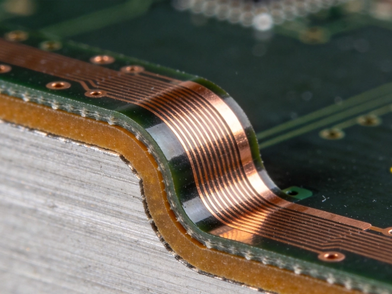
Common DFM Mistakes in Rigid-Flex PCB Layouts: A Comprehensive GuideJuly/29/2026
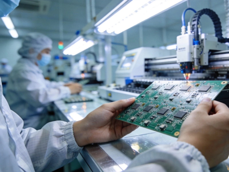
What to Look for in a Reliable SMT PCB Assembly Partner in ChinaAugust/11/2026
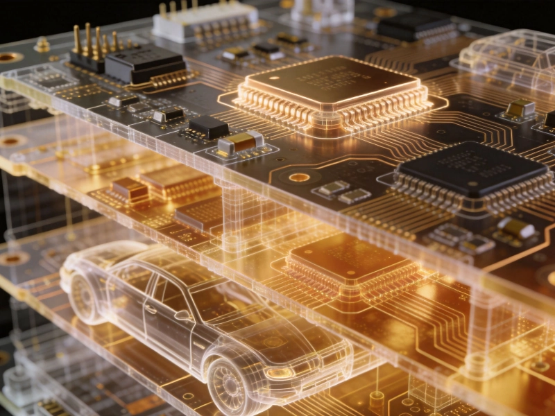
Why Automotive Electronics Demand High-Reliability Multilayer PCBsJuly/13/2026
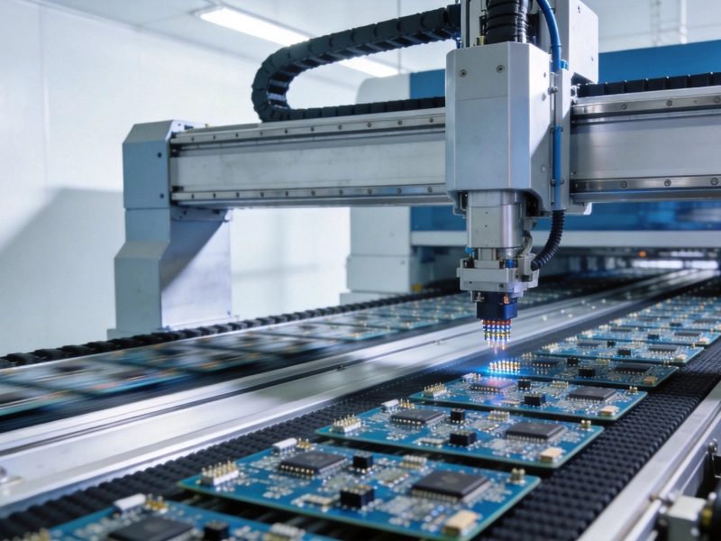
Bridging the Gap: Moving from PCB Prototype to Mass ProductionOctober/09/2026