Open Nav

Implantable medical devices represent one of the most demanding applications in the entire electronics industry. From cardiac pacemakers and neurostimulators to cochlear implants and drug delivery pumps, these devices operate inside the human body for years—sometimes decades—without any possibility of physical maintenance. The printed circuit boards at the heart of these devices must deliver extraordinary precision and unwavering reliability, because a single failure can have life-threatening consequences.
This article examines the unique Pcb Manufacturing challenges that implantable medical devices present, from material selection and cleanroom assembly to the rigorous testing regimes that ensure every board meets the highest standards of safety and performance.
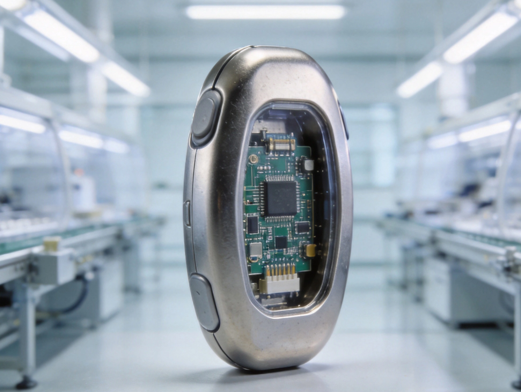
Unlike consumer electronics, where a board failure means a reboot or a warranty claim, implantable devices operate in an environment where repair is impossible and replacement requires surgery. This fundamental reality shapes every aspect of Pcb Design and manufacturing for implantable applications.
The human body presents a uniquely hostile environment for electronics. Body fluids are conductive and mildly corrosive, temperatures fluctuate with patient activity, and constant mechanical stress from movement and muscle contractions can fatigue solder joints and traces over time. Additionally, the device must not generate excessive heat, emit harmful electromagnetic interference, or leach toxic substances into surrounding tissue.
These constraints force manufacturers to adopt processes that go well beyond standard commercial or even industrial Pcb Production. Every material, every process step, and every quality checkpoint must be validated against medical device standards—not just once, but continuously throughout the production lifecycle.
Implantable devices are, by necessity, extremely small. A modern cardiac pacemaker might measure just 50 millimeters in length, with the PCB occupying a fraction of that volume. This extreme Miniaturization pushes PCB Fabrication to the limits of current technology.
Trace widths and spaces on implantable device PCBs routinely reach 3 mil (approximately 75 micrometers) or finer. Some advanced designs utilize 2 mil traces, demanding laser direct imaging (LDI) rather than conventional contact printing to achieve the required resolution. Layer-to-layer registration must stay within ±25 micrometers across all layers—significantly tighter than the ±50 micrometer tolerance acceptable for most commercial boards.
High-density Interconnect (HDI) technology is essentially mandatory for implantable devices. Microvias with diameters of 4 mil or less enable the interlayer connections needed to route complex circuitry within an extremely limited board area. Sequential Lamination builds—often three or more build-up passes—allow designers to pack functionality into an ultra-thin form factor. The via plating process for these Microvias requires electroless copper deposition followed by electrolytic plating to ensure reliable, void-free fills that will not degrade over the decades-long expected service life.
Many implantable devices include wireless communication capabilities for telemetry and programming. Impedance-controlled traces must maintain tight tolerances—typically ±5% or better—to ensure proper RF performance. This demands not only precise dielectric thickness control during lamination but also careful selection of substrate materials with consistent and well-characterized dielectric constants.
Material choices for implantable device PCBs must balance electrical performance with biocompatibility and long-term stability inside the body.
Standard FR-4 is rarely suitable for implantable applications. Its epoxy resin system can absorb moisture, potentially leading to delamination or conductive anodic filament (CAF) growth over extended periods. Instead, implantable PCBs typically use high-performance substrates such as polyimide or specialized low-absorption epoxy systems. These materials offer superior dimensional stability, lower moisture absorption rates (below 0.1% by weight), and better resistance to the thermal cycling that occurs during sterilization processes.
Copper traces must be protected from the body's corrosive environment. Electroless nickel immersion gold (Enig) is the most common surface finish for implantable PCBs, providing a solderable surface while protecting the underlying copper from oxidation. However, the nickel layer must be carefully controlled to prevent "black pad" defects—phosphorus-rich nickel that can cause solder joint embrittlement and eventual failure. For the highest-reliability applications, electroless palladium immersion gold (EPIG) offers an even more robust alternative.
Lead-free solder alloys, mandated by RoHS regulations, present particular challenges for medical reliability. SAC305 (Sn96.5/Ag3.0/Cu0.5) is widely used, but some implantable device manufacturers opt for SAC305 with added dopants (such as bismuth or antimony) to improve thermal fatigue resistance. The solder alloy must also meet biocompatibility requirements, since any leaching of metallic ions into body tissue is unacceptable.
Contamination is the enemy of reliability. Even microscopic particles—dust, fibers, or ionic residues—can create latent defects that may not manifest for years but can eventually cause catastrophic failure. This is why implantable Pcb Assembly must take place in a controlled cleanroom environment.
Assembly of implantable device PCBs typically requires ISO Class 7 (Class 10,000) cleanroom conditions at minimum, with critical processes—such as die attach and wire bonding—often performed in ISO Class 5 (Class 100) environments. These facilities maintain strict controls on airborne particle counts, temperature, humidity, and electrostatic discharge (ESD) levels.
Even after cleanroom assembly, boards must undergo ionic contamination testing per IPC-TM-650 Method 2.3.25 or equivalent. Residual flux ions, if left on the board, can cause electrochemical migration between closely spaced conductors—a slow but relentless process that can eventually create short circuits. Implantable devices typically require ionic contamination levels below 1.56 micrograms per square centimeter of NaCl equivalence, significantly cleaner than commercial electronics standards allow.
Many implantable device assemblers use no-clean flux systems to eliminate the risks associated with cleaning processes (entrapment of cleaning agents in under-chip spaces, for example). However, these flux systems must be thoroughly validated to confirm that their residues are genuinely benign and will not degrade over the device's expected service life. This validation involves extended temperature-humidity-bias testing, often running for thousands of hours to simulate decades of in-body operation.
Manufacturing PCBs for implantable devices is not simply a matter of applying best engineering practices—it is a regulated activity governed by multiple overlapping standards and regulatory requirements.
In the United States, the FDA's Quality System Regulation (QSR), codified at 21 CFR Part 820, establishes the requirements for the methods used in—and the facilities and controls used for—the design, manufacture, packaging, labeling, storage, installation, and servicing of finished medical devices. Every PCB manufacturer producing boards for implantable devices must operate under a Quality Management system that complies with these requirements.
The international standard for medical device Quality Management systems, Iso 13485:2016, is often the baseline certification that OEMs require from their Pcb Manufacturing partners. This standard goes beyond Iso 9001 by adding requirements specific to the medical device industry, including design controls, process validation, traceability, and risk management throughout the product lifecycle.
Risk management per ISO 14971 is integral to implantable device development. Every potential failure mode of the PCB—from a cracked via to a delaminated layer—must be identified, analyzed, and either mitigated to an acceptable level or justified as residual risk. This analysis drives many of the manufacturing controls and test requirements that implantable PCB manufacturers must implement.
The testing regime for implantable device PCBs is far more extensive than for any other application. The goal is not merely to catch defects but to demonstrate, with statistical confidence, that the board will perform reliably for its intended service life.
Flying probe or fixture-based electrical testing verifies continuity and isolation on every single board produced—not just a statistical sample. For implantable devices, 100% testing is non-negotiable. Additional functional testing verifies that the board performs its intended circuit functions correctly, often at the operating temperature extremes specified for the device.
Thermal cycling tests, typically per IEC 60068-2-14, subject boards to hundreds or thousands of temperature cycles to simulate the thermal stresses of years of in-body operation. Humidity testing per IEC 60068-2-78 exposes boards to elevated temperature and humidity conditions to accelerate any moisture-related failure mechanisms. Combined stress testing—simultaneous thermal cycling with electrical bias—provides the most realistic simulation of actual operating conditions.
For BGA and QFN components common in implantable device designs, automated X-ray Inspection is essential to verify solder joint quality beneath the component where visual inspection is impossible. Advanced 3D computed tomography (CT) scanning can reveal voids, head-in-pillow defects, and other hidden anomalies that 2D X-ray might miss. These inspection systems must be qualified and their detection capabilities validated against known defect samples.
Highly Accelerated Life Testing (HALT) and Highly Accelerated Stress Screening (HASS) push boards well beyond their specified operating limits to uncover design and process weaknesses. HALT identifies the fundamental limits of the design, while HASS provides a production screen that catches any boards with latent defects before they ship. For implantable devices, HASS profiles are carefully developed to provide effective screening without consuming an unacceptable amount of the board's useful life.
If an implantable device fails in the field, the manufacturer must be able to trace every component and process step back to its origin. This traceability serves two critical purposes: it enables targeted recalls that affect only the potentially defective population, and it supports root cause analysis that prevents similar failures in the future.
PCB manufacturers serving the implantable device market must maintain records that trace each board to specific material lots (laminate, Copper Foil, solder paste, flux), process parameters (reflow profile, lamination temperature and pressure), equipment used (specific machines, their calibration status, and maintenance history), and operators involved. These records must be retained for the device's expected lifetime plus a regulatory-mandated additional period—often 15 years or more.
Serialization of individual boards, typically through laser-marked 2D data matrix codes, enables this granular traceability. Some manufacturers are now implementing blockchain-based traceability systems to provide an immutable, independently verifiable record of every step in the Manufacturing Process.
Selecting a PCB manufacturer for an implantable medical device is a decision with profound implications. The wrong choice can result in regulatory delays, costly quality problems, or—worst of all—patient harm. Several factors should guide this critical decision.
The manufacturer should have a documented track record of producing boards for implantable or other life-critical medical devices. Experience with consumer or even industrial electronics, while valuable, does not adequately prepare a manufacturer for the rigor and documentation burden of implantable device production.
Verify that the manufacturer operates cleanroom assembly facilities meeting ISO Class 7 or better, and that these facilities are properly monitored and maintained with documented environmental control records. Cleanroom certification alone is not sufficient—ongoing operational discipline is what matters.
Iso 13485 certification is a minimum requirement. The manufacturer should also be prepared for—and experienced with—customer and regulatory audits. FDA auditors, Notified Bodies, and OEM quality teams will all scrutinize the PCB Manufacturing Process, and the manufacturer must be able to demonstrate compliance with every applicable requirement.
The manufacturer must possess the technical capabilities required by the design: HDI Sequential Lamination, microvia formation and plating, fine-pitch SMT placement (01005 components and 0.4mm pitch BGAs), and advanced inspection (X-ray, CT, Aoi). Equipment capability studies (Cpk analysis) should demonstrate that all critical processes are well-centered and capable of consistently producing within specification.
Implantable device development requires close collaboration between the OEM and the PCB manufacturer. Process changes—any changes—must be communicated in advance and formally approved. The manufacturer should willingly share process data, capability studies, and quality records. A partner who resists transparency is a partner who cannot be trusted with life-critical production.
Manufacturing PCBs for implantable medical devices sits at the intersection of advanced electronics technology and life-critical responsibility. The precision required to fabricate ultra-miniature boards with fine traces and microvias, the reliability demanded by an application where failure is not an option, and the regulatory rigor that governs every aspect of production—all of these factors combine to create one of the most challenging manufacturing environments in any industry.
Success requires more than just capable equipment. It demands a manufacturing culture that prioritizes quality above throughput, a quality management system that ensures complete traceability, and a testing regime that verifies reliability to statistical confidence levels appropriate for life-critical applications. For medical device OEMs, choosing a PCB manufacturing partner that embodies these values is not just a procurement decision—it is a patient safety decision.
As implantable medical devices continue to advance—incorporating more functionality in smaller packages, adding wireless capabilities, and extending expected service lives—the demands on PCB manufacturing will only intensify. Manufacturers who invest in the capabilities, certifications, and culture required to serve this market will find themselves at the forefront of one of the most meaningful applications of electronics technology.
Ready to discuss your implantable Medical Device Pcb requirements with a manufacturer who understands the stakes? Contact our team to learn about our ISO 13485-certified facilities, cleanroom assembly capabilities, and track record of serving life-critical medical applications.
Introduction to Flexible Printed Circuit Boards (FPC): Beginner's GuideMay/18/2026

Flexible PCBs in Modern Cars: Sensors, Displays, and Comfort SystemsSeptember/01/2026
What is Flexible PCB? Complete Guide from China Flex PCB ManufacturerMay/18/2026

Top 5 Advantages of Using Rigid-Flex PCBs in Modern ElectronicsAugust/07/2026
Introduction to Flexible Printed Circuit Boards: A Practical Engineering GuideMay/18/2026
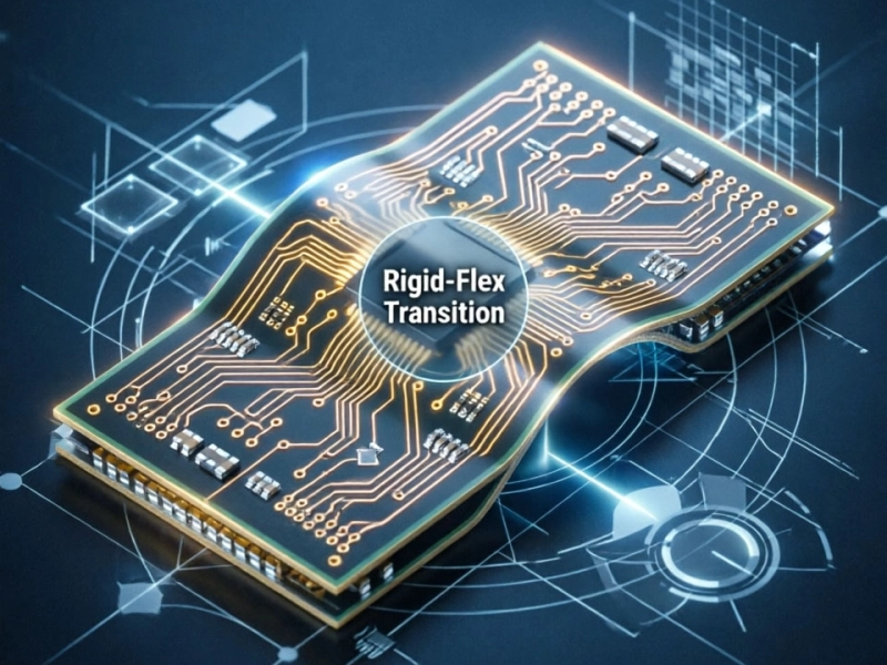
Rigid-Flex PCB Design Guide: Bridging the Gap Between Rigid and FlexJuly/03/2026
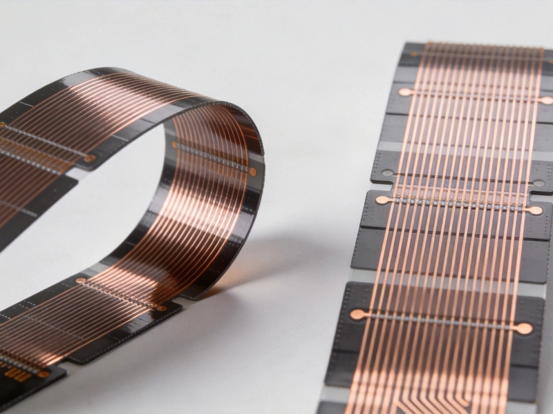
Dynamic vs. Static Flex: Which FPC Type Fits Your Project?July/20/2026
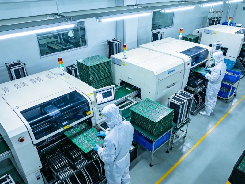
Behind the Scenes: A Tour of Our State-of-the-Art PCB Factory in ChinaMay/19/2026